The next stage of the reflow oven project is moving to a custom PCB for the controller electronics. Overall the board is based on the ATmega32u4 with a DS3231 RTC. The LCD module is intended to be driven by one of Adafruit’s Serial backpacks. There is an area of LED indicators (something I learned from a previous project) and some extra VCC/GND pins sprinkled about.
The following resources compliment my EAGLE Introduction Classes and eBook. Files mentioned in those resources will be provided here, although, the original creators may have newer versions available.
EAGLE Tutorials
These are EAGLE tutorials I have created. There is a mix of written and video content.
-
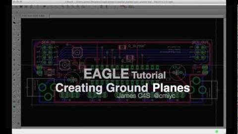
Groudplanes (video): https://www.baldengineer.com/blog/2012/07/25/eagle-ground-plane-polygon-fills/
-
Creating Split Names: https://www.baldengineer.com/blog/2012/12/26/creating-split-net-names-for-eagle/
-
Copy and Paste (video): https://www.baldengineer.com/blog/2013/03/01/eagle-tutorial-copy-and-paste/
Creating PCBs in Eagle is a straight-forward process once you understand how EAGLE works. In fact, most users can get up to speed enough to draw a Schematic and then layout a simple PCB. Making the connections between components is not only fun but can be a form of artwork.
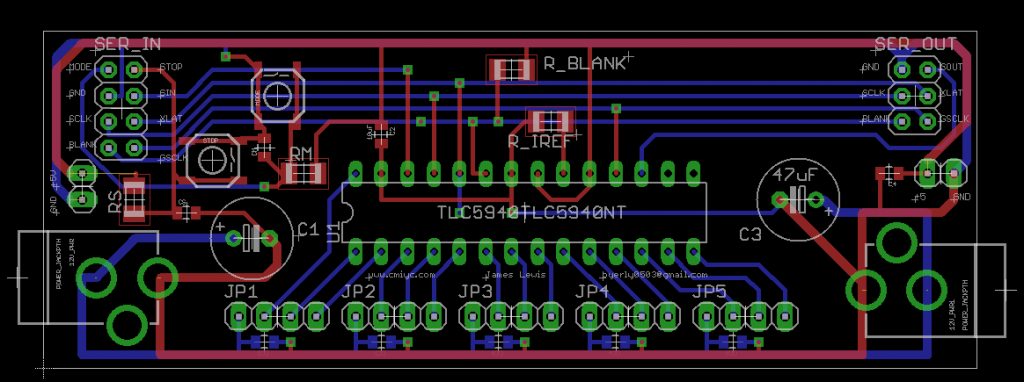
Often overlooked is how much space is left wide open. For example, a board might look like this:

The area in black will have no copper. For circuits that don’t require a ground plane, this may not be an issue. However, it rarely hurts to fill in empty area with a ground plane. EAGLE makes it very easy to do this, after your circuit design is complete.

This screen shot is an all-layer view of my TLC5940 painter board. The 1st draft featured two TLC5940s, but I decided it made the board too large. Instead, I wanted the ability to mount the painter boards around the LED’s shadow box. This should make routing all the wires much easier.

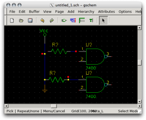
In an attempt to find a free set of schematic and PCB tools for hobby work, I looked back at gEDA. The last time I used it was when the project first started, years and years ago. I was happy to see that OS X had a set of fink packages for the gEDA suite. After figuring out how to get X11 in Leopard (since I didn’t include it when I installed 10.5) and install fink, getting gEDA going was a snap. The user jluciani in the Arduino forums has provided some free pcb footprints he has used from previous projects.


