
A new project I have started working on involves the Apple IIgs. It was Apple’s last 16-bit (and 8-bit) computer. Inside are many application specific integrated circuits, or ASICs, that make the IIgs an extraordinary member of the Apple II family. One chip, in particular, is called the “MEGA-II.” This chip takes all of the individual logic chips from the original Apple II design and incorporates them into a single 84-pin PLCC.
The project I have in mind needs the MEGA-II. I need to design some printed circuit boards for it and a few other IIgs chips. That goal means I need at least one custom Kicad schematic symbol. I plan to create a custom library of Apple IIgs components.
Like other computers from the same era, complete schematics are available. However, they are not in a modern format. Since I need to create symbols for so many of the chips as it is, I may end up re-creating the entire IIgs schematic.
For now, here is the process I use to create custom KiCad schematic symbols and parts.
Difference between KiCad Footprints, Symbols, and Libraries
KiCad has a separate library for schematic symbols and PCB footprints. The only place that a linkage between the two occurs is in your project. In the schematic editor, you can define a footprint to associate with a schematic symbol, or component.

For example, I have a file named “My_Schematic_Library.lib” and a folder named “My Footprint Library.pretty.” Let’s take a look at what makes up these two KiCad libraries.
Schematic Symbol Library
A schematic library consists of three files: .dcm, .lib, and .bck. KiCad creates the .bck automatically. In case you make unintended changes to your library file, you can roll-back to the previous version.
The .dcm file contains metadata for the library’s symbols. The .lib file contains all of the schematic symbols as a “library.” By the way, the file format is plain text, so you can quickly view or edit it.
Cache
Within your project folder, KiCad creates a file called “-cache.lib.” It keeps all of the symbols used in a schematic. With this file, any computer can open the schematic.

The KiCad schematic symbol library and the cache is a single file. Next, let’s look at how the PCB library differs.
PCB Footprint library
PCB footprints are also text files that have a “.mod_kicad” extension. A directory of these files makes up a PCB library. The directory name has, for lack of better term, an extension. That extension is “.pretty.” How cute is that?
If you see KiCad files with the “.mod” extension, those are legacy PCB footprints.
Since there is one PCB footprint per file, it is possible to have multiple footprints for the same component. So for example, if you have an 8-pin and 10-pin footprint for a microcontroller in the same library, there could be two separate .kicad_mod files. Meanwhile, you might have a single schematic library file which has two components defined in it with an 8-pin and 10-pin variant.
The rest of this post is on how to create a custom schematic symbol. For footprints, I am a fan of using existing footprints when possible. KiCad has a vast library of standard footprints that are easy to match up to a custom schematic symbol.
Step #1. Create a schematic library
Creating your library keeps your custom symbols in one place. These can be symbols you create or download. (By the way, do not forget about services like SnapEDA when you need symbols or footprints.)
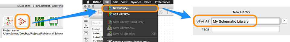
Start in the KiCad project manager. Click the “Symbol Library” icon. Once it loads, go to File and Select “New Library.” Give your library a name and location. For reference, I keep mine in a Dropbox folder so I can sync between my laptop and desktop.
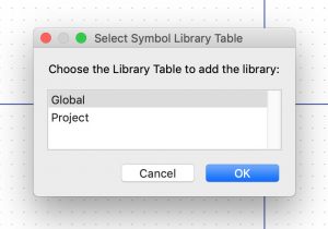
Next, you need to tell KiCad if you want to keep this library specific to the current project or if you want it available globally. Global means all projects can access it.
Add an existing KiCad Schematic Library
If you already created a schematic library file, you can “Add Library” and then select Global or Project.
Step #2. Create a custom KiCad part
These details are the bare minimum you need to create a usable custom KiCad schematic symbol.
2a. Create a new part
Click the “New Part” Icon.
KiCad first asks which library to make active. If you do not see your library, go back to the previous step to create it or add it to your configuration.
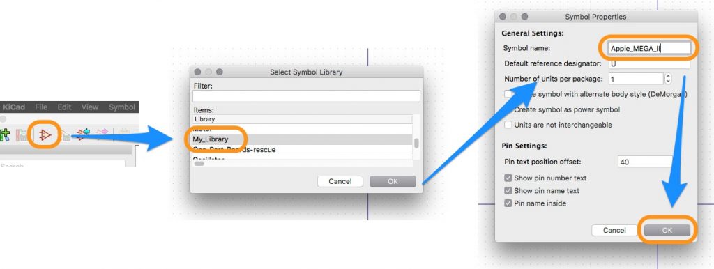
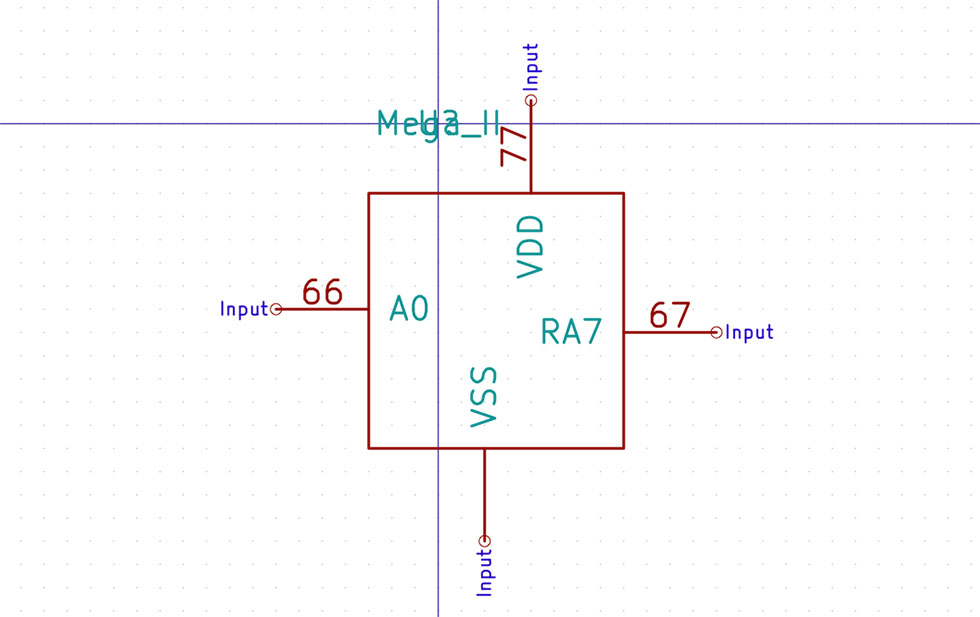
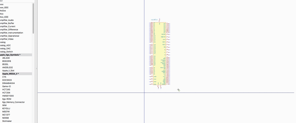
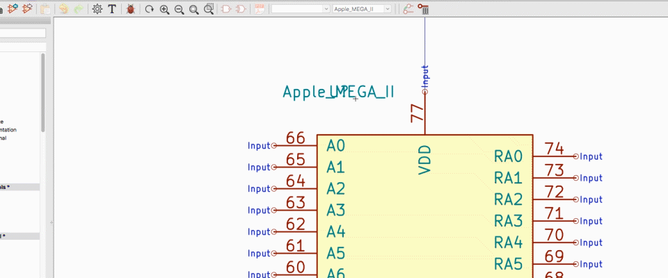
Give the Symbol an appropriate name. In my example, I used “Apple_MEGA_II.” Next, Kicad creates a bare minimum symbol with the name and designator piled on top of each other.
By the way, you could also open an existing part by double-clicking one from the list on the left.
2b. Add Pins
Next, you need the most critical aspect, a component’s pins. KiCad gives you many attributes to describe a pin, but there are 3 requirements:
- A Pin Name,
- The Pin Number, and
- It’s Orientation.
Note, I say requirements above. However, you can create pins without either a name or pin number.
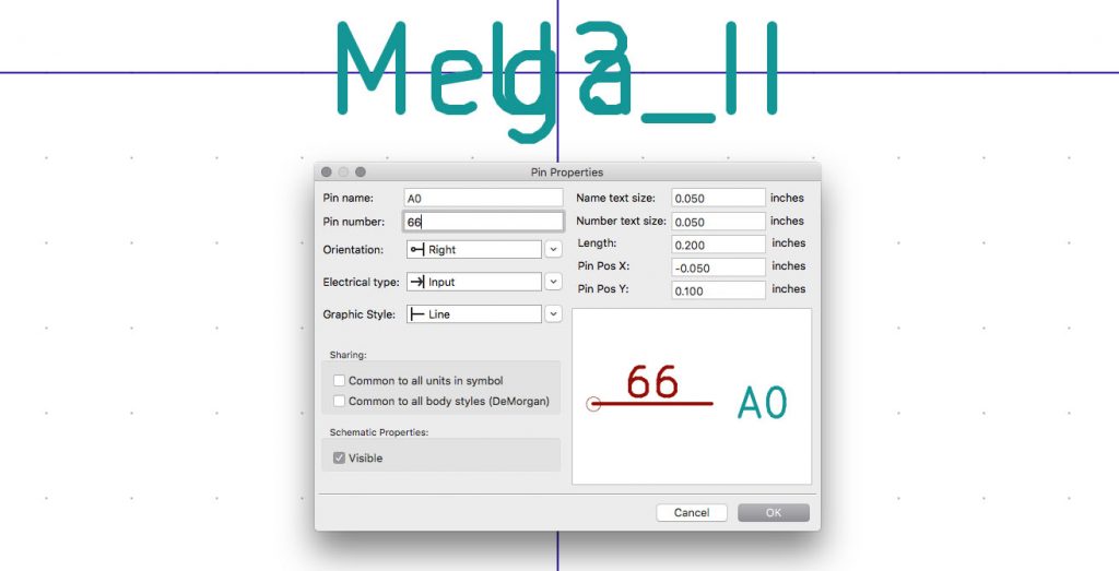
The name should be descriptive. If you use the tilde (~) character, KiCad adds a bar above the name. This mark is useful for inverted or active-low signals.
If your symbol has multiple package styles, you need to create a different symbol for each style to match up the pins’ numbers.
The orientation lets you place pins on all of the sides of a symbol. I find the names “up, down, left, right” backward. After exiting the dialog, if you need to change the pin’s orientation, use the ‘r’ hotkey.
One optional element is the pin’s function.
You can define the function as input, output, power, and several others. This extra information s used when running the Electrical Rule Check (ERC). It tries to detect schematics with short circuits. I rarely set that value. By the way, ground should be a “power input.” Why? Well. That is the subject of another post.
Pin Layout strategies
When laying out the pins, I know of three strategies:
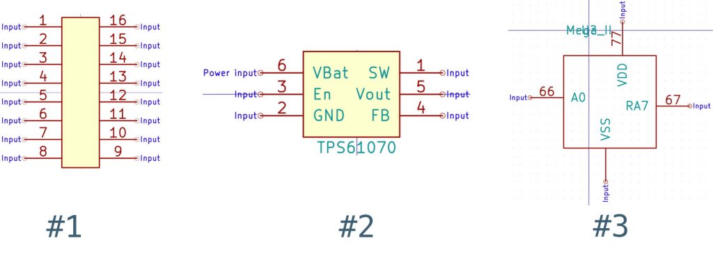
- Pin Order. This method is similar to setting up the schematic as the IC or component appears. So if you were making a 7400 NAND gate, pins 1 to 7 would be on the left and 8 to 14 on the right.
- Schematic Order. I don’t know a better way to describe this one, except, you design the part for the intended schematic. The best example is when I use the TPS-series of switching regulators from TI. I create symbols that look like the example schematic. That way when I add the inductors, capacitors, and resistors, I see a nice clean schematic.
- Chaos. If you choose to do so, you don’t need to follow any logic at all. Hey, it is your library, I do not judge. Well. At least until you ask for my help.
The most popular method I use is #2. If necessary, I create custom symbols for a schematic so that the project schematic stays clean.
2c. Draw a shape
After you make your pin layout, draw a rectangle—or whatever shape is necessary— to close out the symbol.
A little bit of housekeeping that I like to do is to grab all of the elements and move them to the center of the editor window. My goal is to place the 0,0 of the editor at or near the center of the custom KiCad part.
2d. Adjust Designator and name
Lastly, make sure the name and designator labels are in an appropriate place. My convention is to put the designator at the upper-left hand corner and the name field at the lower-right hand.
This point is an excellent time to make sure the designator makes sense. Are you drawing an IC? Then you probably want the letter U. However, if you were drawing a passive component (L, C, R), a discrete transistor (Q), or a connector (J) you may need to pick something else.
Step #3. Save the part
Saving the part updates your custom KiCad schematic library.
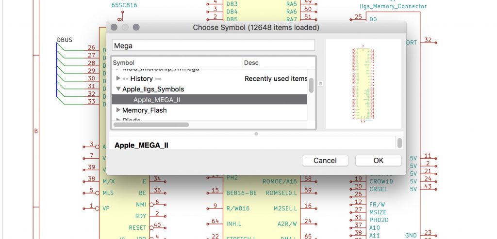
Step #4. Use the part.
Jump over to the KiCad Schematic (aka EESchema), then drop in your part and you are good to go.
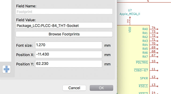
Step #5. Connecting to footprints
I am not covering how to make custom footprints in this post. However, let’s take my example of the Apple MEGA-II. It is an 84-pin chip. The default footprint-libraries that come with KiCad cover most of the standard component footprints. Searching through them can be a bit difficult, or at least, overwhelming. Here’s the trick I use: Google it.
For example, I searched “KiCad Github PLCC 84″ and found the following results.

Looking at the GitHub repository, I can see that “Packages_LCC.pretty” contain the footprint I need. So then when I edit the footprint in the schematic editor, I go to Packages_LCC and grab the PLCC 84 footprint.
Conclusion
Following this simple guide, creating custom KiCad parts is quick and simple. As I mentioned, these are the minimum required steps. In the “Add Pin” dialog, there are more options you can define, which make for a more robust definition. It is up to you.
In the meantime, I am going back to drawing the Apple IIgs schematic.


2 Comments
Hey James, nice post! I recently downloaded a copy of Kicad and went through their tutorial. I’m looking at using it to design a board for a personal project in the not-too-distant future.
I noticed a small detail up near the top of your article. In the image just above where you said “A schematic library consists of three files: .dcm, .lib, and .bak.”, it looks like the 2nd file is called My_Schematic_Library.bck rather than .bak. Is that a typo, or did Kicad change up the extension for their back-up file?
Hey Karl! I need to look deeper into it. It looks like KiCad5 makes a .bck, but older versions made a .bak. Not sure what is going on yet.
BTW. Moving from EAGLE to KiCad is a bit of a change. I think KiCad’s schematic editor is significantly faster once you learn the shortcuts. The PCB editor, though, is a bit rougher. Once you get past all of its quirks though, I think you’ll like it better.
For me, understanding that schematic symbols and component footprints were handled separately was the biggest “ah-ha” moment.