
A common task for a transistor is switching a device on and off. There are two configurations for a transistor switch: low side and high side. The location of the transistor determines the type of circuit and its name. Either transistor configuration can use a BJT or MOSFET.
In this post, I draw the configuration for both transistor types, discuss which requires a driver, and explain why you would use either. If you are new to transistors, check out the resource links at the bottom. I have a few videos I made and some from element14’s The Learning Circuit, which do a great job introducing transistors.
Low-side transistor configuration
When the transistor is connected to ground, that means the load is between +V and the transistor. Since the transistor is switching the path to ground or is sitting on the low side of the load, it is called a low-side switch.
Typically these use an NPN BJT or an N-Channel MOSFET.
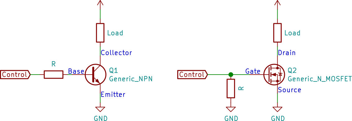
For an NPN BJT, the emitter connects to ground, and the collector attaches to the negative side of the load. As a switch, the BJT operates in saturation mode. Saturation means there is enough base current to turn on the transistor fully.
For an N-Channel MOSFET, the source connects to ground, and the drain connects to the negative side of the load. While you can use a JFET for this circuit, an enhancement mode MOSFET works better.
High-side transistor switch
The opposite of the low-side switch is the high-side switch. This transistor connects between +V and the load. Because of how transistors work, these can be a little more difficult to use in an Arduino or Raspberry Pi circuit.
Typically these use a PNP BJT or P-Channel MOSFET.
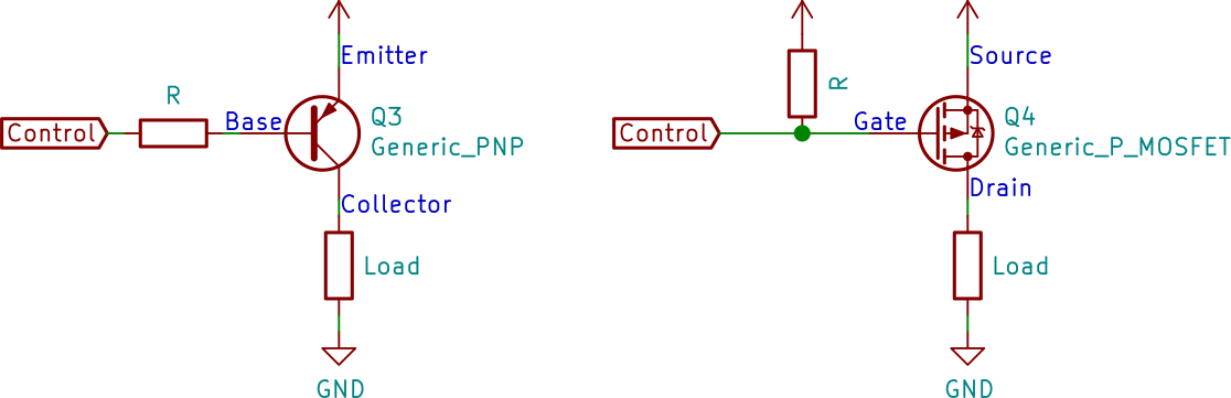
For a PNP BJT, the emitter connects to the voltage source, while the collector connects to the load’s positive side. Looking at the schematic drawing for an NPN and PNP, the PNP might look like it is upside down. Like the NPN, the PNP BJT must operate in the saturation region to turn on the transistor fully.
For a P-Channel MOSFET, the source connects to the voltage source, and the drain connects to the load’s positive side. Like with the low side, you probably want to use an enhancement mode MOSFET. Keep in mind that you may never find a depletion mode P-Channel. They only exist in textbooks and as data entry errors.
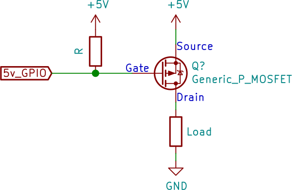
The circuit above works fine when using a P-type transistor on a load voltage that is the same voltage level as the signal driving the transistor. Well, the logic is inverted but other than that, it is fine. For a detailed explanation, check out my post on P-Channel MOSFET Tutorial with only Positive Voltages.
You need a driver when the load voltage is HIGHER than the signal voltage. Next, let’s see how a driver gets used with low-side and high-side transistor switches.
Transistor driving another transistor
A driver transistor circuit is one that controls another transistor. This circuit is not the same as a BJT Darlington pair, which is a high-gain BJT. Instead, a transistor driver is used when the driving signal’s voltage (or current) is incompatible with the load transistor. Below are two cases where you might need to use a transistor driver. These are, by no means, the only ones. So if you know of a case, or suspect you need one, leave a comment with it.
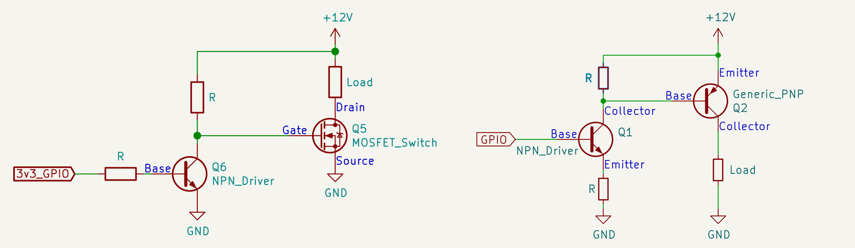
High current MOSFETs have a substantial Vgs threshold. While 5 volts from an Arduino GPIO pin might be enough to turn on the transistor, it isn’t enough to drive it into saturation. Until the FET is saturated, its Rds-ON can be relatively high, limiting the maximum current it can handle.
Note: A common mistake is saying “For a switch, drive a MOSFET into saturation.” This is NOT the case. It turns out, saturation for a MOSFET is different from saturation for a BJT! (Their definitions are swapped!)
In a MOSFET operating as a switch, you want it to stay in the linear (or ohmic) region.
(I’ve updated this post, because I accidently said the wrong thing…)
Using an NPN driver with a PNP BJT or P-Channel MOSFET is very common when the load voltage is higher than the signal voltage. Without a driver, the transistor may never turn off. The driver effectively boosts the driving voltage high enough to unbias the Vbe or Vgs junction of the transistor. My tutorial on PWM a PC fan is an example of an Arduino driving a 12 volt fan with a PNP.
Why even bother with high-side transistors?
For both BJT and MOSFET transistors, their P-Type generally have more resistance (or lower current capability) than their N-type counterparts. For that reason, some might conclude you should always use an N-type in a low-side configuration.
However, step back and think about what the two different circuit types are doing. The low-side switch is switching ground while the high-side switch is connecting the voltage supply. Generally, you want to keep the ground connected in a circuit and switch the power. One reason is that even when the transistor is fully turned on, there is still a small voltage drop across it. That voltage drop means the ground is not 0 volts for that device. It does not matter which you switch for something simple like an LED. However, an active device like a Microcontroller needs its ground to be ground! So when you have a load that requires ground, you NEED to use a high-side switch.
As a quick rule of thumb, a low-side switch is a simple solution if you turn a device on and off. However, if you are delivering power to an entire circuit or a voltage-sensitive device, then you want to use a high-side switch.
By the way, there are off-the-shelf components called “load switches.” These ICs have a P-Channel MOSFET as the switching transistor with a built-in driver for that P-Channel. There is no external driver needed for this type of component.
Transistor Basics Links (for Reference)
- The Learning Circuit, How Transistors Work. Karen explains from the ground up how bipolar junction transistors (BJTs) operate. There are many transistor physics explanations on the web, but Karen’s is the clearest one I have encountered.
- The Learning Circuit, BJT Feedback. In this TLC episode, I joined Karen and addressed some misconceptions from the community (and I suspect others) on the video linked above.
- AddOhms, BJTs. The video I made about BJTs. I don’t get into how the electrons work, but instead, I show how to use one in a circuit.
- AddOhms, MOSFETs. Part two of my transistor videos. In this episode, I explain how to use MOSFETs.


70 Comments
Nice explanation. You clearly explain the high and low sides switches, and clearly have a lot of knowledge and experience to share. Thank you for explaining when to use each. It makes sense to switch a microcontroller load using a P-ch MOSFET. And that’s generally easy, because the voltage level will likely be near the one doing the switching.
But it would be good to hear your take on how to switch much higher loads using a P-ch mosfet Are there alternatives to using a bootstrapping capacitor to drive the gate from a much lower voltage, such as 3v driving 24V?
Small clarification, you don’t want to operate MOSFETs in their saturation region when using them as switches. You use them in their linear and cut-off regions.
I’m making this clarification due to this paragraph that I’m quoting down below:
“High current MOSFETs have a substantial Vgs threshold. While 5 volts from an Arduino GPIO pin might be enough to turn on the transistor, it isn’t enough to drive it into saturation.”
Good catch. I cannot believe I wrote that! I always correct others for saying the same (wrong) thing. Thank you.
Hi! Great article about using FETs in various configurations. I can’t find a solution for my scenario. Maybe it’s because of my lack of understanding. I have to switch (PWM) a 12V power (I<1A) LED, but with active_low 3.3V TTL from GPIO0 of an ESP8266-12E. I'm bound to switch on low-signal, because all other GPIOs are already in use. I like to know whats the best circuit todo so?
This page link JUST got copied to my desktop. Thank you for explaining these subtleties in straight english. I have been doing hobby electronics for decades but never messed with MOSFET or driving inductive loads with them. I have spent weeks trying to peel back the veil and stop burning up components and all the other sites only explained like you already know half the ossues. Thanks again for going right to the heart of it. I
Most helpful and informative article I’ve come across in my effort to convert my Chevy’s dashboard to dimmable LEDs 🙇🏼♂️ Thank you!
I want to control a 14 segment common anode display using an Arduino. In the code, I also want to write a HIGH to the segment pin to turn it on. As I understand, I will need a low-side switching circuit for each segment. Am I on the right track?
Yes. You would put the switch between the cathode and GND. Don’t forget a current limiting resistor for each segment (unless you plan on multiplexing them.)
Thank you for the reply. Do you have a tutorial on multiplexing? My display is in fact a dual 16 segment common anode display 🙂
I built the second Transistor Driver example, but I think it has an issue. If you switch on the NPN on the left, what limits the current flowing from Vcc, into the PNP, out of the base, through the NPN and info ground – there doesn’t appear to be a resistor in this path.
Hi!
The NPN transistor’s current limiting resistor limits the base current, which means that the collector current is inherently limited. The collector current is also the PNP’s base current. Thus, the one resistor effectively limits the base correct for both transistors.
Took me a while to understand that, too 🙂
Thank you for this tutorial. The quick reference to load switches was also helpful. It ended up leading me to a TI site -> https://training.ti.com/load-switches-vs-discrete-mosfets on the topic.
For your right example of the NPN driving the PNP, how do you know the value of the resistor at the top?
1k
I’m using P-channel mosfets to control the anodes on rows of an RGB LED matrix. N-channel mosfets control the cathodes. It’s an 8×32 matrix that works fine when Vdd is 5 volts, but when the voltage is raised to about 8 volts (I need 12 volts to light the LEDS brightly), other rows other than the ones I chose come on. I.E. all rows are on when I just want the top two. I’m using an Atmega328 and 74LS138 decoder to select one of the 8 rows with each o/p tied to the gate of the Pchannel fet.
So, to reiterate: if voltage is 8 volts, the same rows light up but then so do all the rest in the same columns. I know it has something to do with the Vgs but my attempts to pull the voltage down to 5 volts with NPN transistor with/without zener diode, have failed. The mosfets are FQU11P06, Vgs between 2 and 4 volts. I think some calculations may be in order.
The gate to source resistor is 10k ohms I’ve looked at some of the images/schematics on this page, but mine don’t work that way! I had breadboarded my design (~500 points on a PCB) but had the voltage turned down to 5 volts during testing because at +12 they were too bright and blinding me! My bad, because it works NOW at 5 volts but not at 12 volts.
Have you looked at some of the Arduino libraries for LED matrices?
A particularly good one is by Majic Designs and goes under the name of Parola – both names would find the library on Github.
The Arduino Forum is a good source of information as well.
I guess you had a look at the MAX7221 chip which is specifically designed for driving matrices up to 8 of 8×8.
So, I have a 12v 555 circuit that the output triggers a 12v lamp…..I installed a 2N2222 on the low side. The collector is at pin1 on the IC, the base is from a 5v trigger and the emitter connects to the 5v and 12v ground. Where there is not 5 volts triggering the transistor, the output on pin3 on the IC is around 4 volts. Do I then have to scrap the low side switch and do a high side switch? Use the emitter on the to make connection to pin and 8 on the IC?
The description doesn’t make a lot of sense.
Can you add a circuit diagram and how you are using the 555?
Pin 1 on the IC, I presume the 555, is ground – the collector of the NPN would not be connected to ground.
The base of the transistor, if you are using the 555 to time, needs to be on the 555 output.
Firstly, I would use the 7555, not the 555, then test the transistor part of the circuit separately from the timer.
The 555/7555 takes a negative-going pulse on its trigger, the output is a positive-going pulse that goes to the transistor base.
Low side switching would be fine for switching a lamp – what type of lamp? LED or filament?
I am switching a LED and or Buzzer rated at 12v. How can I add an image or my schematic? I am a first time caller.
You will need to ask the administrator.
Usually, a simple hand-drawn sketch will do, photograph it and add or insert it as a png or jpeg file.
If you can do it, draw it as it is connected.
You still need to tell the readers exactly what you are trying to achieve, because all anyone can deduce at the moment is that you have a timer, an LED or buzzer and a transistor and that possibly the timer controls the transistor and the transistor turns the LED or buzzer on and off.
Why don’t you set up a simple circuit with the transistor wired as a low side switch, emitter to ground, base through a resistor and switch to a positive voltage, collector to your LED, limiting resistor for the LED and the positive side of the LED to your 12-volt supply.
You can measure voltages at the transistor collector pin relative to ground.
https://drive.google.com/file/d/15FS-APcvonCFTUC3BinXoUSevNWhd88r/view?usp=sharing
Link has been released from filter.
The end game is that I want to use a RX480 to trigger the circuit on.
Forget end games.
You still haven’t explained what you are trying to do, and now you throw something else into the mix, a radio?
I’m out of here.
I did explain. I want to trigger the 12v timer circuit with a remote. The RX480, once triggered has an output voltage of 5v. I want to use that to trigger a 12v circuit on or off. The 12v circuit is a timer that turns on a 12v lamp/buzzer in a pattern that is manually changed by flipping the SPDT switch to the corresponding resistors.
I see why id doesn’t make sense…..my link to the schematic image has not been posted.
The right schematic of the “Transistor driver examples” will go up in smoke, you need an extra resistor!
Hi! If you read through some of the comments, including mine, you’ll find that no additional limiting resistor is needed. The PNP base current is the NPN emitter-collector current. Therefore, when you calculate the NPN limit resistor using Ohm’s law, the current will be the PNP base current divided by the NPN hFE.
This took awhile to sink in for me (pun intended).
Very helpful tutorial. Thank you!
Hi, I was doing a project, where I need to heat up a nichrome wire (which acts as a heating element) upto certain power for example 100mW. I have already done some computation and I need current of approximately 0.05A. I was planning on using a BJT current driver to limit the current at a constant rate. Since my current requirement is lower than 1 A, I thought of using BJT as it will be a better option than using MOSFET. But I am getting a little confused if MOSFET could be a better choice. Can you suggest what will be better?
How do you plan to keep a constant current and presumably a constant temperature?
Most applications like this will use Pulse Width Modulation (PWM) to maintain a steady current with some sort of temperature sensor.
You could use either a BJT or a MOSFET as the driven device.
I use a P-channel MOSFET driven by a BJT to control the speed of a circulating fan.
MOSFETs make excellent switches. You just need to pay attention to the Gate voltage. For low voltage applications, say 5-volts, you need to select a MOSFET with a logic-level Gate voltage
Thanks Philip, however PWM only controls the Voltage right? How will it control the current?
With PWM, the voltage remains the same.
What does change is the time the voltage is high against the time the voltage is low.
This is the mark-space ratio which varies from 100% – always on – to 0% – always off.
When driving a resistive load like yours, the current will follow the voltage as dictated by Ohms Law.
PWM changes the power applied to the load.
Imagine it as applying 12-volts to a DC motor. Switching the voltage rapidly takes the motor to full power then turns it off.
The apparent speed will be dictated by momentum and inertia.
At very high frequencies, you don’t notice the slowing down and speeding up.
With my fan, it speeds up and slows down exactly as if you were varying the voltage.
With your wire, if the mark-space radio is low, the wire is cool; if high, the wire will be cool.
When I said steady current, I should have said average apparent current.
If you have a temperature sensor, it will control the PWM ratio or duty cycle.
You can only really do PWM with an MCU like Arduino.
A lot will depend on how accurately you need to control the temperature.
Someone might come up with a simpler solution
Thanks for this tutorial! I’m trying to use a PNP transistor, driven by an NPN transistor. As I mentioned in my response to STiVo, I discovered that directly connecting the NPN collector to the PNP base blows the NPN transistor. I put in a 3K resistor, but I always have current flowing, and the load is always powered. I tried adding a pullup resistor between the PNP base and +12V, then I tried a pullup resistor between the NPN collector and +12V. Neither of those did anything. Any suggestions on how to track down the problem?
It would be helpful if you said what transistors you are using.
My old faithfuls are NPN 2N3904 and PNP 2N3906.
Double check all the transistor leads against the datasheets (the 2N39xx are always from the left, Emitter, Base, Collector looking at the flat face of the TO92 package with legs down).
For the transistors mentioned, I always use at least 10k on the base.
Persevere with the configuration in this article because it does work.
Let us know how you get on so others can benefit from your experience, good or bad.
Sorry, I did mean to mention the transistor types. They are 2N3904 and 2N3906. I’ll try increasing the resistors. Thanks for the tip!
No harm if you protect both bases with 10k, but I’ve never blown a transistor if you follow the datasheet pinout.
Make sure you have some sort of load on the PNP or you will blow the driven transistor. An LED with 2k would work safely up to 12-V. The 2N39xx’s are medium power. A 10k on the load side would give you a voltage to look at with a meter.
Out of interest, which one did blow?
It turns out both of them blew. The PNP blew a hole in the casing, but the NPN just silently failed. I think that was what caused my later problems.
My test load is an LED with a 1K resistor (12V supply voltage, Vce 0.25V, 2V drop measured across the LED, I calculated that would draw 9.75 mA)
After letting the Magic Blue Smoke out of 3 or 4 more transistors, I finally got a configuration that worked. I used a 30K pullup for the PNP, and a 10K on the NPN base. And the NPN collector was directly connected to the PNP base, with no issues.
Next step – see if it works with my intended load, not just an LED! But that’s for another night.
(Note to self – pick up a Magic Blue Smoke Refill kit 🙂 )
Correction to my previous comment – the NPN blew a hole in the casing and the PNP silently failed.
Thank you for your post.
You well explained how to drive a P-Channel mosfet with a BJT. But what if the load supply voltage is above maximum allowed VGS of the mosfet? For example if we want to switch 50 volts, when the IO signal is zero, the BJT is off and so the gate is at 50 volts while the source is at ground 0 volt. so the 20 volts max VGS is exceeded.
How can we prevent that?
(sorry I asked the same question in another post, just saw this post and thought my question is more relevant to this post)
Do you use bypass capacitors on your low side configuration?
Hi, James!
Thank you so much, very helpful. But suppose I want to use a p-MOSFET high switch to turn on/off +3.3 volts from a PSU, but the only voltage available for driving signal is +5v. Will that scenario even work? BTW, both +5v (driving) and +3.3 come from the same PSU.
In your transistor driving another transistor example, when the NPN is switched on, won’t there be unlimited current between the base of the PNP and the collector of the NPN?
I can attest that yes, the current is unlimited 😀 Lovely sparks from the NPN transistor, though!
That’s why I have lots of spares 🙂
I retract that statement, because I did manage to get the circuit working properly without a resistor between the two resistors.
In fact, I observed, that the current seems to be very high (didn’t measure though). I’m using a BC547C (NPN) and a BC557C (PNP). When turning the NPN ‘on’, everything works as expected, only the NPN was rapidly getting hot.
I’ve added an additional resistor (2.2k) between the PNPs base and the NPNs collector and everything is fine now!
@James Lewis: Great tutorial! It helped/helps me a lot, to read the articles on your site!!
Remember NIXIE tubes are suppose to be driven by <60% duty AC. You can use DC if you keep the duty down to an integral of <60% duty. But due to the abruptness of the PWM duty control you will need to periodically exercise the tube. And more often longer the displayed number is kept static.
Can you explain why I have occasionally seen an n-channel MOSFET being “controlled” by its source pin? In this configuration its gate is fixed at 3.3V and its drain is connected to the gate of another NMOS. That NMOS is pulled up to 10V at the gate. This driving MOSFET is trying to turn that NMOS off. Its the same setup you have shown above except instead of using a BJT its using an NMOS and the NMOS seems rotated to me!?
Source pin is connected to an MCU.
I would need to see an example or a schematic. I’m not sure why a gate would be tied to a voltage and the source pins be left disconnected.
I have a picture but i’m not sure how to post it here. Do people typically put it on a website and provide a link?
I’ll try this
https://drive.google.com/file/d/1S2ruQnUJ-eBPcyZHZ_OSYsTHFwS3T_2w/view?usp=sharing
I don’t know why would configure the transistors like that. I’ll have to think about what the advantage is, but at first glance, I don’t see it.
The circuit on the top right will be on before anything else. And when it comes on Q1A should come on automatically. The micro will eventually disable that using the sideways FET.
That MOSfet is being used to protect the MCU. Think of it a low DSr diode. With a threshold of 3.3V
Thank you for this article, James.
With regards to the left-hand ‘Transistor Driver Example’ (NPN transistor driving N-Channel MOSFET), how do you compute the values for the two resistors?
Neither value really maters. 1 Kohm would work fine for both.
thanks a lot for this detailed info
Outstanding! I’ve been searching for information such as this. Specifically, an inverter circuit/NOT gate, (I think,) controlling a relatively high voltage nixie tube for displaying “00” when idle. (The tube is part of a pair, to indicate GPIO triggers from 01 to 16.Sort of a side-project for work. Someone needed a way to test the GPIO portion of an A/V system. “Hey, sounds simple, I could do that!” Silly me!)
Thanks for sharing your knowledge!
-Mike
Thanks for this great info! I’m learning a lot.
I have a question in your description of the high-side switch. You mention that for the P-Channel MOSFET, the drain connects to the voltage source, and the source connects to the load’s positive side. This is the opposite of what your diagram shows. Is this a mistake in your text description?
Looks like I made a bit of a mistake. The diagram is correct, the text was not. I’ve fixed. Thank you for letting me know.
Perhaps your new video can demonstrate the “sourcing/sinking” question. Thanks
Can you explain what you mean about sourcing/sinking? (Something beyond what those terms mean?)
Shouldn’t this read collector attaches to the negative side of the load?
For an NPN BJT, the emitter connects to ground, and the load attaches to the negative side of the load.
Thank you. I fixed it.
Great tutorial for those of us just learning as we make things. I am in the middle of controlling a siren using an Arduino and IRL520 MOSFET. I was wondering about some of the possible configurations and the logic of using one over the other, you answered the question, well done.
I have seen some circuit diagrams that use a 10k pull-down resistor on the Gate while other s omit it. Is this resister good practice or unnecessary?
Steven
Depending on when you looked, I updated the diagrams to include pull-down and pull-up resistors on the MOSFETs. A MOSFET gate is such high impedance, that a resistor is helpful when you need to force it to a known state. The most common example is a GPIO pin. At first, you might think, “well it will always either be high or low.” That is true. Except for IO pins, on every MCU I know about, start in a high-impedance state. So there is a short period of time where the MOSFET’s gate is effectively disconnected. In those cases, a pull-up or pull-down resistor is a good idea.
The same could be said for BJTs. Most BJTs have enough leakage current that they naturally stay off until a voltage is applied. However, a pull-up or pull-down should be considered.
you need connect resistor between base and emitter (also between gate and source) . Imagine, control pin disconnected.
Always useful to have another explanation of these. I have to look it up every time.
Just started dabbling with FETs. I needed one to drive a circulating fan in a fridge by Arduino PWM so it ramped up and down according to temperature,
I also needed to drive a relay with the output from a sensor (HCPL3760) that has an output low on current sense. The relay needed high side switching. A P-channel FET did the job nicely with no additional components. I’ve see references to holding the gate high with a pullup resistor going to Vcc. I guess you don’t leave the gate floating?
Hey James, I spotted you put a resistor on the base and gate connections of the transistors. How do you calculate the values of these for each of the difference circuits?
Thanks so much! This is a succinct and clear explanation.