Creating PCBs in Eagle is a straight-forward process once you understand how EAGLE works. In fact, most users can get up to speed enough to draw a Schematic and then layout a simple PCB. Making the connections between components is not only fun but can be a form of artwork.
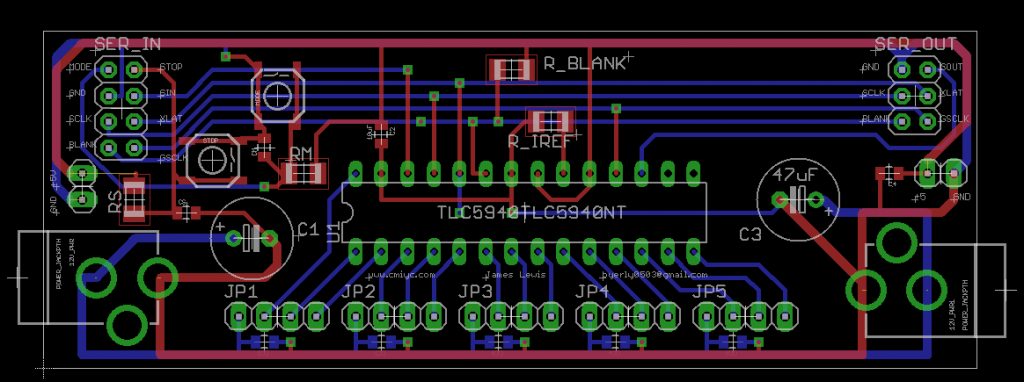
Often overlooked is how much space is left wide open. For example, a board might look like this:

The area in black will have no copper. For circuits that don’t require a ground plane, this may not be an issue. However, it rarely hurts to fill in empty area with a ground plane. EAGLE makes it very easy to do this, after your circuit design is complete.
Step 1. Create your PCB
My suggestion is to not worry too much about how to fill your empty spaces with a ground plane. Simply lay out your board as cleanly as you can. [Note. This advice is for low-frequency circuits with content well below 1MHz. For high-speed layout, certain rules must be used.. So, lay out a board.
Step 2. Draw a Polygon
Once a board has been designed, using the POLYGON command, draw a rectangle (or whatever shape you wish) around the perimeter of your entire board. Do not worry about holes, but you should follow your (20) Dimension Layer if you have an unique shape to your board.
Using the INFO command highlight your new POLYGON and select the (16) Bottom layer.
Step 3. Give the Polygon a Name
Right now your new POLYGON has a NAME that EAGLE has assigned to it. Change the name of the POLYGON to GND using the NAME command. When prompted select “this Polygon”.
Congrats, you have just created a ground plane, isn’t it beautiful. Wait, something is wrong. The board looks like it did before. Hm. EAGLE will not fill in the POLYGON until you run the RATSNEST command. So click that now. And ta-da we see a ground fill in the printed circuit board.
EAGLE will not fill in the POLYGON until you run the RATSNEST command.
Step 4. Isolate!
There doesn’t look like much space between the traces and the ground plane. This might cause issues when manufacturing the boards. So let’s increase the isolation area a little bit by using the INFO command. Personally I like to use 0.016, but your mileage may vary. If DRC gives clearance issues, increase the Isolation a little bit.
While in this window, make sure the “Thermals” box is checked. This box will give some thermal relief around ground pins and vias that connect into the plane. Without this thermal relief, it will be very difficult to solder to the pad, since the ground pour will act as a huge heat sink.
Step 5. Don’t forget the top layer
Now go back and repeat steps 2-4 for the top layer.
Step 6. Add some Vias
One of the important things about having two ground planes is they need connection points. So sprinkle a couple of Vias around the board and change their NAME to GND. On through-hole boards this is less important, but always helpful.
Exercise for the Reader
Doing these simple steps before generating your Gerbers will result in more professional looking boards, and in some cases, may even result in a most robust PCB design. Something I like to do on my boards is to keep the bottom layer’s POLYGON solid while making the top layer’s POLYGON “hatched”. This is done in the Properties window (INFO command) and selecting a different type of Polygon Pour.


11 Comments
You might add that it is environmentally friendly to use a ground plane, since much less copper has to be chemically removed from the board via some nasty etchant chemical such as ferric chloride.
Great video as an introduction to the use of polygons.
A few tricks you can add;
– Before routing the board enter in the command line “ratsnest ! gnd” . This will remove the yellow un-routed lines for the ground signal. In some cases it makes life a lot easier! (If you want to see all signals again, use “ratsnest *”)
– When clicking on the polygon button, you can enter the signal name in the command line. So in this case you would click on the button, enter “gnd” and draw the polygon. Once the polygon is closed (finished) you can immediately draw another one, but if you want to name it, you have to enter the name in the command line.
– After the first via, use the name button to rename it to “gnd”. Then use the copy function to copy the via, which will then automatically retain the “gnd” name. Beware: When copying groups of vias you will always end up with a new name.
One small warning; When you have removed the unrouted ground connections using the “ratsnest ! gnd” command, you will not see the unrouted gnd signals ever. That means if your gnd polygon is not covering all gnd connections, you might end up with unrouted gnd connections. Check therefore always the statusbar after clicking the ratsnest button! It will tell you if this is the case. And if it does, use the “ratsnest *” command to show the missing connections..!
Very cool tip. I had no idea about the !/* arguments for
ratsnest. Thank you.Hey James, Excellent video. This was just what I needed. Thank you. From one bald engineer to another 🙂 – Bruce
Hi James,thanks for the trick!could you please give me a hint on how I can increase trace capacity to support high current like 30A using polygon and stop solder mask layer.I want to to add some 30A Relays on my PCB.Thanks
Very informative. Thank you. I added few things to my board. Hatched ground plane vs solid? I’m confused.
A hatched fill is rarely used for a ground plane.
Hi James, I am very impressed with the quality of content on your blog.
Would you please share your EAGLE files for this circuit?
Hi Marinus,
You can find the original board file here:
https://www.baldengineer.com/?attachment_id=131
That file does not have the polygons for ground planes, but it is the rest of the circuit.
Hi Dave! Awesome that you were able to use the trick. It was really good to see you this week. Look forward to the next time I’m in town. Thanks for the support here and for coming to my presentation.
Awesome trick James. I saw this post when you first put it up and filed it away for that day when I finally had a board that I wanted to send to get made. Well tonight was the night I finally tried it out and it worked like a charm! Nice to see you again today at the Iowa Tech Expo.