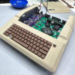
During the component shortage, I got to know Raspberry Pi’s RP2040 microcontroller. It is a dual-core Arm Cortex-M0+ with about 262 kilobytes of RAM. The feature I like most is the programmable IO pins. These are small state machines that run independently of the Arm cores. They allow for some clever tricks. For example, I used them extensively on the Mega IIe project.
This video was supposed to be a project I thought of during the Mega IIe. I call it a state-mode logic analyzer. However, it took me several days to turn on and debug four boards. Time ran out, so I focused the video on debugging custom RP2040-based boards. These are all lessons I have learned from this project, plus about another dozen RP2040 boards I have built over the past couple of years.
Unlike a traditional logic analyzer, a state-mode logic analyzer only stores samples on a qualified clock edge. An example would be capturing 6502 bus traffic on the transitions of the PH0 clock. The advantage of this approach is you don’t need nearly as much memory to capture useful traffic.
I put together an idea for an RP2040-based state-mode logic analyzer to make a long story even longer. The PIO makes it possible to quickly capture all 32 bits of its GPIO pins and DMA that to RAM. That was the easy part. I added a 74LVC245 buffer to provide logic-level translation between the inputs and the RP2040. Then, I added a small counter circuit to create timestamps. Those timestamps are necessary to re-create how much time passed between captures.
The design files for the state-mode logic analyzer are available on GitHub. However, I have had to put the project down for now. I will pick this project up again in the future. However, my current plan is to use the existing boards as a prototype for an FPGA-based tool instead.
Another source for details is the How Hard Could It Be to Debug RP2040 boards post on the element14 Community.


