When your schematic has a large number of related signals, it is helpful to group them. In its schematic editor, KiCad has a few tools to help. Your end-goal helps determine which tools to use. For example, do you need a KiCad bus or a label? In this post, I explore how you can define signals, group them, and reference them across schematic sheets.
Up until recently, I did not need to use a bus or multiple sheets. However, the Apple IIgs project I’m working on is too large for a single page. In a KiCad live stream, I looked at how to create busses and connect them. In a separate tutorial, I will show how to work with multiple sheets in KiCad.
Lastly, if you are not familiar, KiCad is an Open Source eCAD tool. Although I have used others, this one currently my preferred platform.
KiCad Bus, Label, and Wire
Before jumping to how to use a bus, first, we need to start with the basics. KiCad connects nodes with a “wire” element. KiCad gives each wire drawn a unique name unless it connects to an existing node. The user can override the name by adding a label.
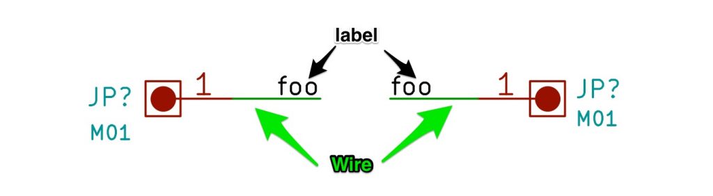
Label
KiCad’s labels give a wire (or node) a human-readable name. Within a schematic sheet, same-named labels connect wires. One advantage of this approach is that it keeps the schematic cleaner. A downside is that typos can prevent signals from being connected.
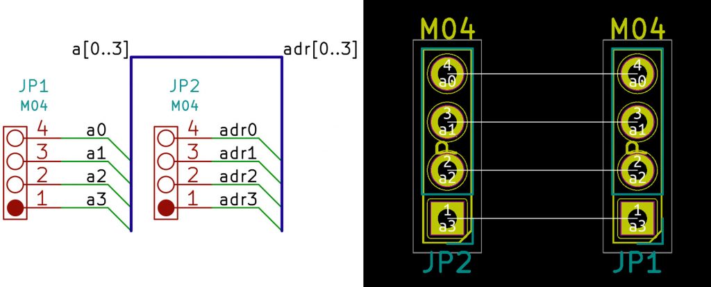
At this point, I am going to show some examples. The two 4-pin headers below represent two components with pins that need to be connected. On the right, I am showing the result in the PCB editor.
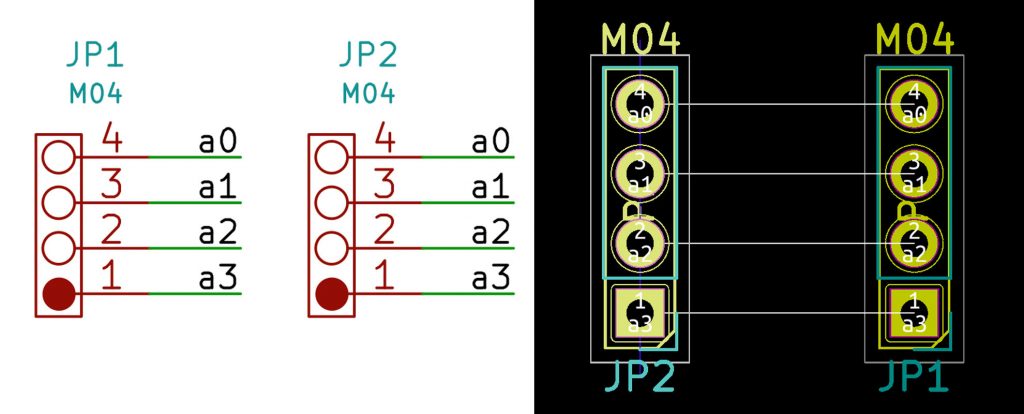
On each header, I extended the wires from the pins and labeled them A0, A1, A2, and A3. In this situation, think of these as a small 4-bit address bus. Since the wires, or nodes, are labeled with the same names, KiCad connects them. The PCB view shows “rats net,” or unconnected nets, between the header pins.
KiCad Bus
The next step up from a wire is a blue line called a bus. However, drawing a bus alone is not enough. First, you must add a “wire to bus” entry, to tell KiCad that you want the wire to be part of the bus. (So far, I have not found a way to edit the direction or length of these “entry” wires.)
So, then what is a KiCad bus?
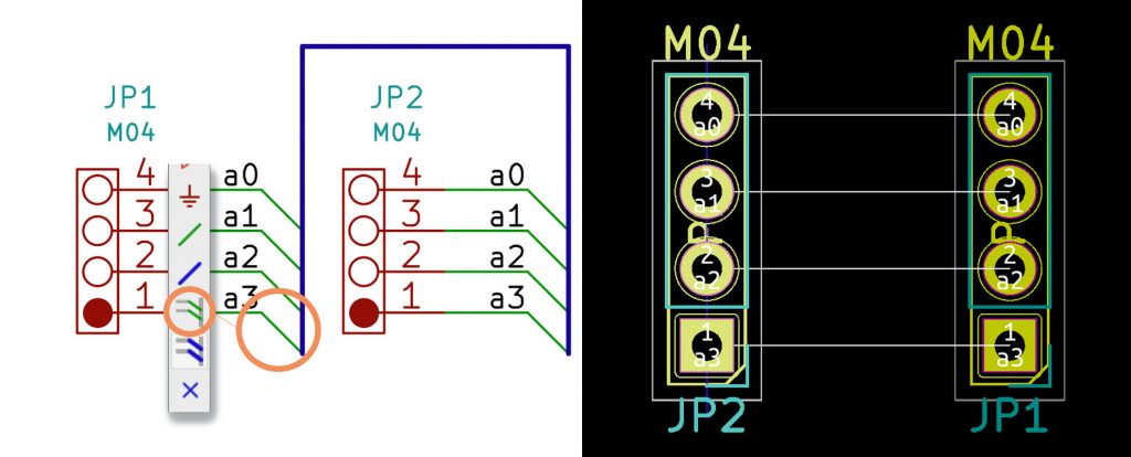
To KiCad, a bus is a collection of wires. For the most part, they are an aesthetic feature. We can connect the connectors from above together with a “bus.” However, this connection does not change anything.
So if the bus is not necessary, what is the point?
Mismatched Pin Names
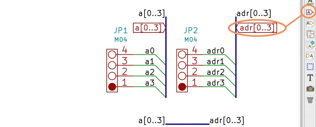
Let’s say you have a different naming convention on one component relative to another. Here, I am changing the right connector to use “adr3” instead of “a3.”
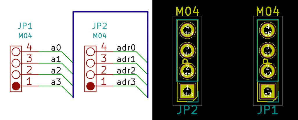
Notice that the connection between the pins is low lost. Since the signals are on the same bus, we can tell KiCad to, effectively, ignore the names and connect the pins instead. The only step necessary is to place a label with each pin group on to the bus, as shown below.
To be up front, I do not fully understand how KiCad makes the mapping work. You could change one of the bus labels to “a[3..0]” but a0 still maps to adr0.
Bus vs. Pin Labels
Take note that you still have to label each of the pin’s wires. KiCad does not figure out pin names when connecting them to a bus. Just like named wires though, you do not have to have a continuous bus connection throughout the schematic. You could create a small segment with both bus names on it. However. One of the main reasons for a bus, versus just a bunch of label names, is making the visual connection.
Local labels vs. Global labels
What if your schematic extends beyond a single page? In the case of my IIgs schematic, it is 9 pages long. Labels and busses are local to the sheet that they are one. But KiCad offers two ways to bring nodes into a hierarchy of sheets.
Global Labels
The first way to bring in labels is with global labels. There are already some defined for you. KiCad automatically shares power labels, such as VCC and GND., throughout a schematic project. In addition to those, you can define Global labels that the schematic project shares across all of its sheets.
The Global Label turns local labels into Global. In the picture above, I have defined both a Local and Global name for adr0 through adr3. KiCad allows Global labels to be applied to a bus as well. Which, in my opinion, is the real power of a bus. Instead of defining a bunch of local and global labels, you can define a global bus.
One of the downsides to the global labels is that they now exist in all sheets. What if you only want to share signals between a couple of pages? What can you do then? In that case, you can use Hierarchy pins to connect signals between sheets.
KiCad Hierarchy Pins
There is one more set of label controls. Within a sheet, you define labels as a hierarchy pin. The name is different because of how hierarchy labels or hierarchy pins work. This feature creates ports into and out of the sheet. For now, I am not going to cover Hierarchy pins. The only point I will make about them is that they can be used to connect signals together between sheets without making signal global.
In a future tutorial, I will break down how to work with multiple sheets in KiCad. At least, for now, you should understand how to create a KiCad Bus which is the tough part.
Conclusion
One of the things that bother me is that on the root sheet look pretty dull. Here is my Apple IIgs schematic. There is nothing there. I did much work to set up each sheet, but this one is just empty boxes. I also feel like setting up wires, pins, and labels are more than necessary.
Video Tutorial
Here’s a Twitch Clip where I worked through this tutorial live. It also shows how to create multiple sheets.
Watch KiCad Labels, Busses, and Hierarchical Sheets (for the Apple


2 Comments
If you press the “r” key, it will rotate the bus “entry” wires.
I do not think you can alter the length of a wire-to-bus entry; however, it can at least be rotated which goes a long way towards making the schematics more aesthetically pleasing to read.