Category

KiCad

Category

One of the last significant steps in a project is designing the custom PCB. This stage means creating a DIY Arduino board that is custom to the application. Two examples of my past projects are BinBoo, a Binary Clock, and Open Vapors, my reflow oven controller.

While working on a project for a friend, I got to thinking; it would be nice to have a checklist for circuit elements to include on a DIY Arduino board. In the early days, I forgot to add a filter cap to AREF, for example.

These tips are based on an 8-bit AVR design, like the ATmega328p chip. You could apply these tips to other 8-bit AVRs. Until now, I have not designed a custom board around a 32-Bit/ARM board. Though at only $16, I would be tempted to just solder the Teensy module directly to my finished board.

Below is a written list of items for a DIY Arduino checklist. If you’d like to see me design this board in KiCad, check out this AddOhms Tutorial.

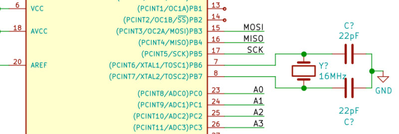
A KiCad BOM is a list of all the parts your design is using. The term BOM, or bill-of-materials, is standard for supply chain management and does not just apply to electronics. KiCad’s eeschema has a BOM export feature. Unfortunately as of Version 4.0, this feature is still somewhat lacking. Given the limitations, here are some tips to take your KiCad BOM from Schematic to Mouser.

Spending a few extra minutes while capturing (drawing) your schematic thinking about your KiCad BOM can save you a ton of time later on. Moreover, as you build up a database of parts, these extra minutes turn into seconds. Here are a couple of ways to describe your parts, especially passive components, better while drawing schematics in KiCad.

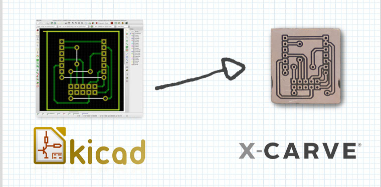
The last time I looked at using an X-Carve for Printed Circuit Boards (PCBs), I created a demo board with EAGLE. Since then, I have learned more about using KiCad, the open source electronics CAD suite. While not a step-by-step tutorial, here is my rough KiCad to X-Carve PCB workflow. These are just the high-level steps, the tools necessary, and the settings I’ve discovered for each—so far.

Eventually, I will make this a more detailed KiCad to X-Carve PCB tutorial, so make sure you subscribe to my RSS feed for updates.

Here’s the Basic Steps:

  1. KiCad: Draw Board
  2. KiCad: Plot Gerbers
  3. KiCad: Generate Drills
  4. pcb2gcode: Generate G-code
  5. Text Editor: Clean Up G-code Files
  6. Camotics: Simulate G-code
  7. ChiliPeppr: Send G-code and control X-Carve
  8. X-Carve: Make the boards!

There are two methods to making a prototype PCB: 1) Etch Your Own or 2) Send to a Prototyping Service. While there are many prototyping service options, most cause you to wait anywhere between 24 hours and 30 days before you get your boards back.

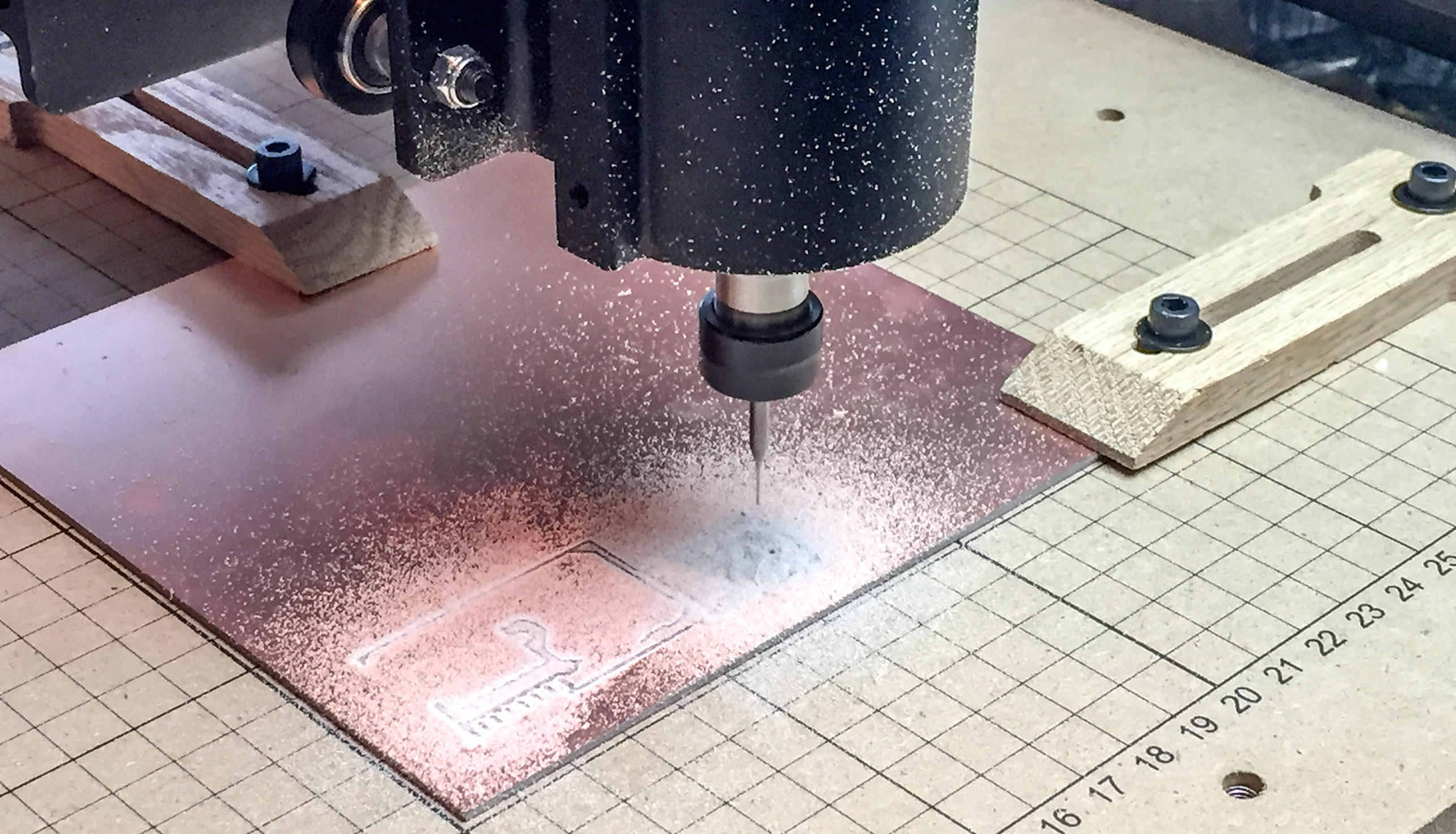
If you need a PCB done today, etching at home is a great option. Chemical etching involves all kinds of steps with all kinds of weird chemicals. If you don’t want your neighbors to think you’re the next Walter White, then mechanical etching is a better option. Which is why I bought an X-Carve from Inventables. It’s a CNC Milling Kit you build yourself.

Keep reading for my X-Carve CNC Review and first-hand experience on etching my first PCB. Plus, lots of pictures!

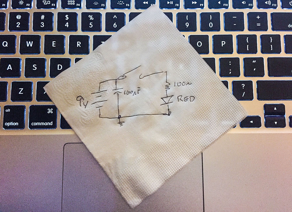
Engineers make a schematic to explain their circuits.

One time I was looking for a non-tourist pub in Japan. I asked someone for help. She said, “I’m sorry, but I do not speak good English. I will bring my friend, and she will draw you a map.” (Exact quote!) The map her friend drew, gave directions to a bar with a “Neon Yellow Sing.” She meant “sign.”

The map was the method we used to communicate with each other, even though we didn’t both speak English. With this crude but useful map, I could find my next drinking place destination.

Schematics are the same as this map. Even if you don’t speak the same language, you can communicate how a circuit works when you make a schematic.

Use one of these five tools, when you need to a document a circuit or when you need to ask for help.