The most popular AddOhms video is my short tutorial on MOSFET basics. In the years since I posted the video, people have sent me many questions. While answering those questions I’ve learned quite a bit as well. For example, in that video, I say that Vgs is the threshold to turn on the MOSFET. Well, it turns out, that is not entirely true. It is the threshold to turn it off! Oops. A minor point with a subtle difference, but a common MOSFET misconception.
In this post, I dispel that and other common myths and misconceptions around using MOSFETs. As with all engineering tips and tricks, this post is not a definitive guide to FETs. Instead, it is meant to be a guide to help you ask the right questions to design in the correct part.
1. Misconception: You don’t need resistors on the gate
Back when I made the AddOhms episode, I added a resistor to the MOSFET’s gate pin. Of course any time a resistor is shown in a schematic, people get worried about what complicated formula is needed to determine its value. For slow switching applications, like below 10 kHz, the resistor value doesn’t matter. Something in the 100 to 1000 ohm range is fine.
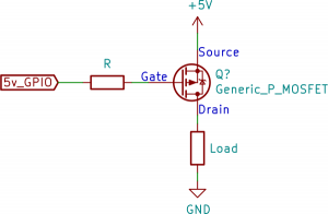
So if the value does not matter, why have one? The gate of a MOSFET is a small capacitor. And what happens when applying a voltage to a capacitor? It starts charging.
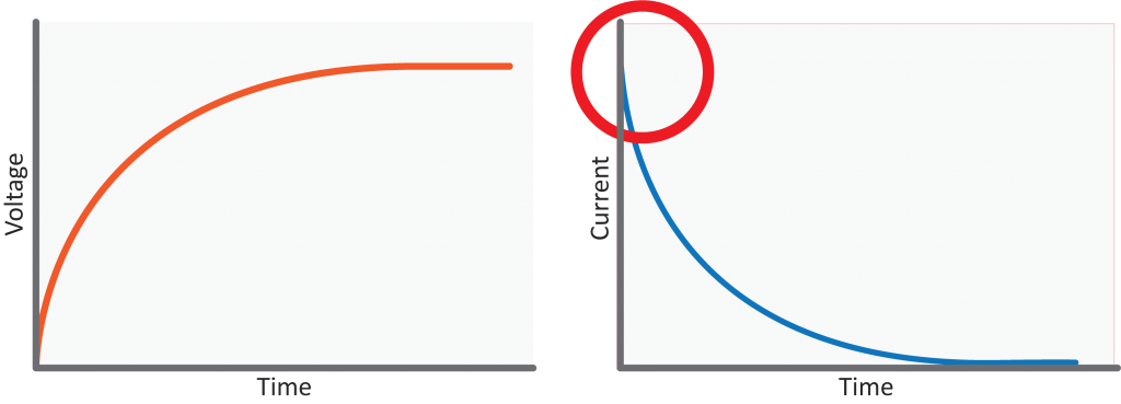
The initial current is very high. It slows down as the capacitor charges. That initial current rush, also known as in-rush current, can be a problem. Even though it is a short time, there is a significant current surge that can damage an I/O pin. Depending on the size of the MOSFET’s gate capacitance, it may not be necessary to include that resistor. I wish I could say to “just” add it any time you use a MOSFET. If there is a high switching frequency, say 100 kHz or higher, then you have to worry about the RC charging curve created by the resistor and the gate capacitance.
Pull-Down (Or up) resistor
Before leaving the resistor topic, there is one more detail I need to add. MOSFET gates are exceptionally high impedance. Just like a GPIO pin set to be an input, a pull-down or pull-up resistor helps keep the transistor on or off during power-on. As a pull resistor, the value is hardly critical, which I explain in this AddOhms episode on picking pull-up resistor values.
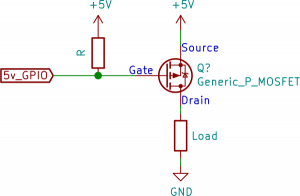
When used with a switch or cable that could be disconnected, it is obvious to use a pull-down or pull-up resistor. Keep in mind, when connecting a transistor to a microcontroller, until the pin switches to an output, the transistor’s gate floats.
2. Myth: Vgs is the threshold to turn on a MOSFET
Fun fact, Vgs is the threshold to turn-off a MOSFET, not to turn it on. At first, this might seem backward. But, consider that the Vgs threshold has a range. The range defines the voltages where the FET transitions between “on” and “off.” So the Vgs value is when it turns off.

When a MOSFET “turns on” it becomes active. When active, the resistance between the drain and the source varies. That resistance depends on two things: Vgs and Id. Id is the drain current. But I’ll get into that more in the next section. Here, I want to explain: why does Vgs have a range? For the FQP30N06L, Vgs(th) is between 1.0 and 2.5 V. What do those numbers mean?
Here is the best way to look at the Vgs range. In this example, the max Vgs threshold is 2.5 volt. The datasheet tells us if the gate voltage is at least 2.5 volts higher than the source voltage, the transistor will be active. Like most components, manufactured transistors have variation. The datasheet range states that the FET may turn on with as little as 1.0 V. However, it is guaranteed to be active with at least 2.5 V. The other way to look at this value is that anything below 1.0 V turns the transistor off.
While Vgs tells us when the transistor turns on (or off), it does not tell us much else about its behavior. We have to look further into the datasheet for that.
3. Misconception: MOSFETs are variable resistors
Even though transistors get used for switching applications, they are much more complicated than a switch. In the case of MOSFETs, they have three regions you need to understand: cut-off, linear and saturation. In the cut-off region, there is no current flowing between the drain and source. In other words, it is off. The other two need a bit more explanation and a graph. Let’s look at the on-region characteristics for the FQP30N06L.
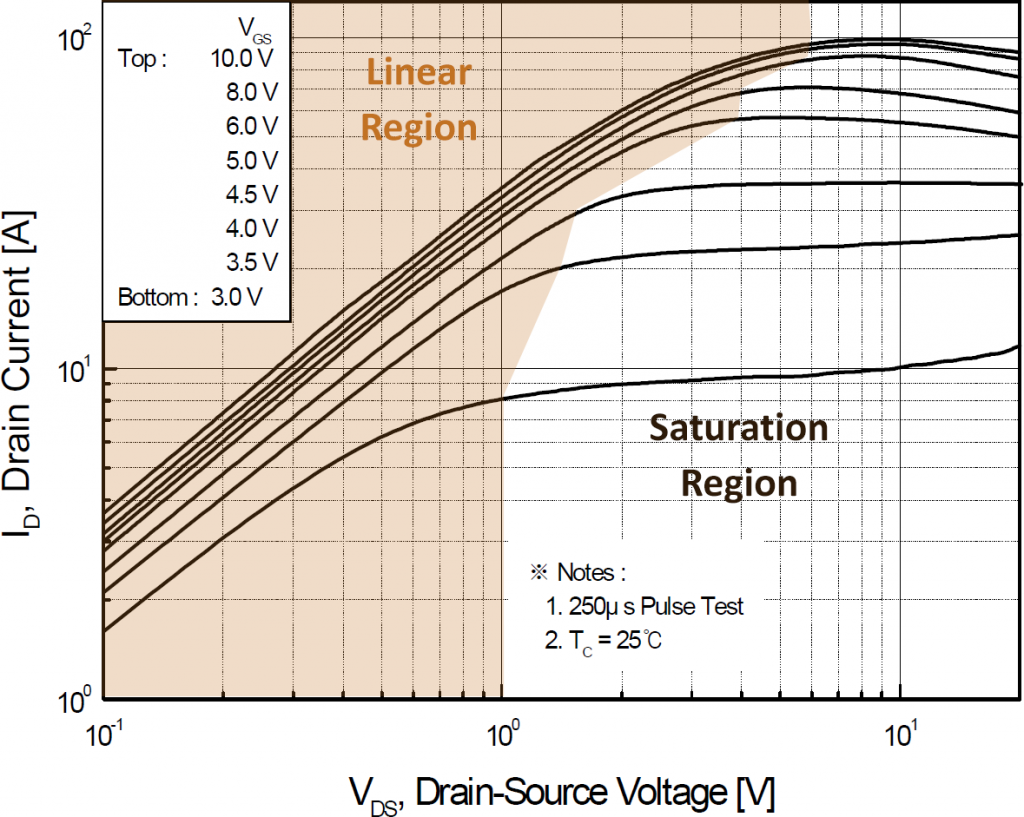
The graph shows several pieces of information. It shows the MOSFET’s drain-source voltage drop (Vds) and drain current (Id) based on the gate-source voltage drop (Vgs). See I told you it isn’t a simple switch. One point I want you to notice is that there are multiple curves for different Vgs values. So while this MOSFET works with about 2.5 V, it is barely turned on. It is designed, like many MOSFETs, for a higher Vgs.
Now, let’s look at those two active regions.
Linear Region
The area highlighted in orange is called the “linear region.” Why? Because the drain-source voltage (Vds) is proportional to the drain current (Id.) Take away the subscripts, and you get V divided by I. Sound familiar? (Hint: It’s Ohm’s Law.) The linear region is sometimes also called the ohmic region.
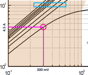
Here is an example of when the Vgs value is 3.0 V. The purple line shows that when the drain current is about 4.5 A, the voltage drop from source to drain is 300 mV. At this highlighted point, the resistance from drain to source (Rds) is approximately 66 milliohms. That is almost twice the advertised value of 35 milliohms. (At 4.5 A, to get that magic 35 milliohm, you need a Vgs of at least 5.0 V.)
Also, take note of the blue box. If the drain current is constant at 10 A, then varying Vgs will cause the drain-source voltage drop to change. In other words, the MOSFET is a variable resistor when operated in the linear region.
Saturation Region
The next region is called the saturation region. Notice how the drain current lines begin to straighten out. When the transistor operates in this region, the ratio between the drain-source voltage drop (Vds) and the drain current (Id) does not change very much. While it does vary a little between points A and B in the diagram below, it is basically flat compared to the linear region.
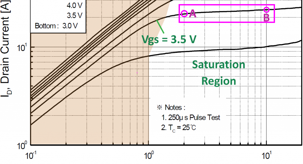
The purple box highlights when Vgs is 3.5 V. At point-A, the Vds is 2.0 V and the drain current (Id) is 21 A. Use Ohm’s law, and you get an Rds around 95 milliohms! With such a high on-resistance, it is not a good idea to drive a MOSFET into its saturation region when used as a switch. If that statement shocks you, then we need to move on to the next misconception.
4. Misconception: Design a MOSFET to use the saturation region
MOSFETs and BJTs define their saturation region differently! A MOSFET acts as a variable resistor in the linear region and as a current source in the saturation region. Unlike a BJT, to use a MOSFET as a switch, you need to operate within the linear region. (BJT switches operate in their saturation region.)
Also, with a MOSFET, there is not an idea of “on” and “fully on.” Once the applied voltage crosses the Vgs threshold, the MOSFET is active. At that point, you can either drive it into its linear or saturation region. There is no “hard” or “full” region. You need to pay attention to your load current and your applied Vgs. From there, you can determine the voltage drop from drain to source and which region the transistor will operate.
If you are designing an amplifier, then you want to drive the MOSFET into its saturation region. Why? Because it becomes a constant current device. The drain current (Id) varies with changes to Vgs. In the linear region, Id relies on Vds changing.
5. Myth: P-Channel MOSFETs require a negative voltage source
Many people look at a MOSFET’s P-Channel Vgs rating and assume they need a negative voltage supply. That is not the case, at least, not very often. Instead, the voltage drop from gate to source needs to be negative. Which is to say the source pin needs to have a higher voltage than the gate pin.
You can find P-channel FETs in high-side transistor switch circuits.
In the past, I’ve written about the myth surrounding negative voltages and p-channel MOSFETs. Voltage drops are relative. So when a data sheet shows a negative value for Vgs, it does not mean a negative voltage relative to ground. Instead, the voltage drop between the gate and the source needs to be negative. For more information, check my post on using positive voltages for p-channel MOSFETs.
6. Truth: All MOSFETs are static sensitive
Have you ever wondered why ICs ship in static protective packaging but components like capacitors or resistors do not? A MOSFET’s gate oxide layer is very thin. It is sensitive to electrostatic discharge (ESD) events. These events are brief moments of intense energy (or is it power?) Most people are familiar with ESD in the form of static electricity. It is essential to understand that semiconductor damage can occur with ESD events that are smaller than what you can feel. In other words, just because you don’t see (or feel) a spark, it does not mean the component is safe. Out of circuit, store MOSFETs in ESD bags. When handling them, wear a grounded wrist strap and work on a grounded surface.
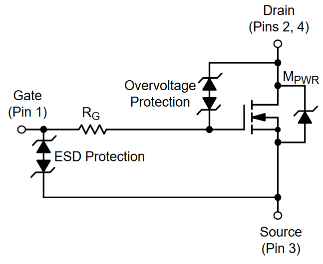
Once in a circuit, MOSFETs still need some protection. A transient-voltage-suppression (TVS) diode protects against transients like ESD spikes. You can also find MOSFETs that feature built-in ESD protection. For example, this ON-Semi 9N05A logic level N-Channel has a protection rating of 5000 V. Look at its equivalent diagram, shown above. There is a diode clamp (structure) between the gate and source to protect from ESD events.
So while some MOSFETs may have protective measurements, the MOSFET structure itself is susceptible to ESD events.
7. Dumb: MOSFETs are better than BJTs
I hate the question “Which is best?” Engineering is not only math and formulas. I define engineering as making trade-offs. So it is not possible to make a blanket statement that “X is better than Y.” Finding the best solution depends on the application. The same statement applies to MOSFETs and BJTs. If one transistor type were best for all circuits, then the other would fade away.
As a general statement, I say that BJTs are suitable for small current and to use MOSFETs for large current applications. When dealing with Arduino or Raspberry Pi level voltages and (relatively slow) switching, this segmentation works well.
Neither transistor is best for all situations. Though, in many applications, you can get away with the wrong one if you are not pushing up against a limit of either technology. But something to keep mind the next time someone asks, “Which is better: a MOSFET or BJT,” is that there is a 3rd option. A device called an insulated-bipolar-transistor (IGBT) is the combination of a MOSFET and a Power BJT. It combines the sharp gate-threshold of the FET with the high current carrying capability of the BJT to combine the best of both worlds. IGBTs are very popular in high-voltage (>200 V) and high current (>100 A) applications. But those are a subject for another post.
For now, if you are not sure if you should use a MOSFET or BJT, then be clear what the application is when asking the question.
Conclusion
Each time I make a tutorial, I realize there are things I didn’t know (or correctly understand.) So my favorite part about this list is that some of these seven MOSFET myths caused me to pull out my textbooks when the questions came in. With each question I get asked, I learn a little bit more. I hope that means I’m about to learn some new things. 🙂 So, what other MOSFET questions do you have? Or, can you share your bits of wisdom about using these fascinating devices? Leave a comment and let us know.


20 Comments
This is an excellent article. Thank you!
Recently I saw a weird design which left the NMOS source opened. Not connected to any terminal.
However, the source still have voltage levels.
Drian has a pull up resistor to 3.3V.
Gate also has a pull up resistor to 3.3V.
I measured the source and it was 2.2V.
When the Drian side becomes 0V, the Source becomes 0V.
Gate is always 3.3V.
(The Vth showed in its datasheet is 1~2.5V)
Do you have any idea why the source is literally “open” but still has the voltage levels?
Thank you very much.
For the inline resistor on the gate of a MOSFET, I would actually recommend a 1kOhm potentiometer when testing it out. I found out the hard way that too much resistance on a gate will drop the voltage too much (luckily I had smaller resistors lying around). If you are using an Arduino, it’s important that you don’t max out the output current on IO pins for an extended amount of time as it will damage it. Experimentally you could get a 1kOhm pot and use a multimeter to test the absolute max your specific MOSFET will actually be able to “activate” this way and then replace the pot with the closest value after measuring.
How to protect to protect the mosfet from di/dt effects?
It’s a very good article, Thanks a lot for that.I am using mosfet for phase dimming project where I am controlling 400W bulb.While turning on Ids peak is going to 30A,because of that mosfet is getting damaged.How to protect the mosfet at the turn-on time.
Good article, thanks. Something that’s bugging me is that MOSFET datasheets seem to have ID graph values well above their stated maximum current (continuous or pulsed), what am I missing? Eg. 2n7000 has maximum rating ID of 200 mAmps. But Figure1 shows ID current up to 1.5A in https://www.onsemi.com/pub/Collateral/2N7000-D.PDF
Hello boys, I’m working on a small project with an IRF1010 mosfet transistor and I hope I can find my wrong, if you have a look into it’s datasheet you will see that its able to withstand a current higher than 80A, however, with a small current of 2A and 12V it gets heat progressively even using a small heat dissipator, I think there is something I’m not considering about it so if you can give me an advice about it I will appreciate it. Cheers
It depends on how you wired it. Are you using it as a low-side switch? If not, the FET isn’t getting turned-on correctly.
You say about pull-down resistor:”Something in the 100 to 1000 KOhm range is fine.” Cannot the resistor be smaller than 100 KOhms?
I believe he meant 100 Ohms to 1000 Ohms instead, those values are awfully high for resistors to basically change the amount of current going into the gate.
Good catch Kaleb. I think I originally wrote “100 to 1kohm.” But didn’t like how it looked, so changed to “100 to 1000 kohm” without thinking! Thanks.
Hi, Thanks for the amazing article.
I would like to know if by operating MOSFET in saturation region, will it damage it or does any of the characteristics change? As per the VLSI text book by Weste and Harris, operating FET in the saturation region will cause the channel to pinch off. And I am also curious to know whether industry operates FET’s in linear or saturation region.
Thanks,
Murali
Hi, thanks for the page; it’s a useful resource to refer beginners to.
(I’d like to point out a small typo towards the end: unless I am mistaken, IGBT stands for “Insulated-Gate Bipolar Transistor”).
Good catch, thank you. I had to read it three times because in my mind I kept reading it as “insulated.” I think I made a Freudian slip when writing the original article. Corrected.
currently says this though: “A device called an insulated-bipolar-transistor (IGBT) is the combination of a MOSFET and a Power BJT.” i.e. missing the “gate”. Small thing but hey typos.
Great Writing Thank Heavens someone spelled it out plainly and with visual concept type information. Your Work is rewarding to many Thanks
nice summary, but I think one point would need more clarification in the form of yet another graph: “Also, with a MOSFET, there is not an idea of “on” and “fully on.” Once the applied voltage crosses the Vgs threshold, the MOSFET is active. ”
There is no sharp on/off transistion and the maximum current a MOSFET can pass is dependent on the overvoltage, i.e. hogh much above the threshold voltage you are. This can bee seen in the ID versus VGS graph shown in every datasheet. This is corresponding to your wording that you can drive the MOSFET into the linear or saturated region, however, I have seen far too many designs were which wasn’t clearly enough understood by the designer.
If you want your MOSFET to carry the current which is typically stated in the headline, such as e.g. 60 A, then you have to apply a high enough VGS to allow for this current to pass.
Esd is also a item for resistors. Read the following. Noting that they are selling expensive resistors.
http://www.vishaypg.com/doc?63129
While making some fast switching drivers, I found that adding a ~10 ohm resistor to the gate would prevent ringing caused by the drain-gate capacitance linkage. (the drain diving to zero volts as the gate was coming up)
On that topic of which is better, I think its important to mention that quite often in switching applications, the power dissipation of a BJT is less than a mosfet for high voltage applications.
Consider a 1A load, at 300V, most BJTs will win over the high RDSon of a high voltage FET.
flipside: Then consider a 40A 24V load, most FETs will win that one.
Hey James, glad you made that point about a resistor for the gate as that got flagged on an article I wrote last month. I made the same point as you, the gate acts like a capacitor so the initial current can be high. It’s also worth checking your microcontroller specs as outputs can often be configured for open drain, open source or push-pull. That would tell you if you need a pull up/down resistor
Nice list and I have to admit the significant of the linear Vs saturation was fully appreciated by myself (more an IGBT user)
The gate resistor is oh so important so I am glad it is here, the peak current is one concern, EMI is another but also the turn-off overshoot (inductive loads) and also inadvertently creating a Pearce oscillator.
The specifics of choosing the gate resistor become more specific with higher power devices and that’s when the list of equations become important