KiCad 8 just dropped. Here’s an AddOhms video covering eight must-try features! The February 2024 release brings a whole host of new stuff to the Schematic editor. However, the PCB editor, CLI, and Simulation tools also received attention. (There are something like 900 closed issues for the 8.0.0 Milestone!) Which of these is your favorite?
2020-04-04: This tutorial is based on KiCad 5. With KiCad 6, the bus feature works a little different (so I’m told.)
When your schematic has a large number of related signals, it is helpful to group them. In its schematic editor, KiCad has a few tools to help. Your end-goal helps determine which tools to use. For example, do you need a KiCad bus or a label? In this post, I explore how you can define signals, group them, and reference them across schematic sheets.
Up until recently, I did not need to use a bus or multiple sheets. However, the Apple IIgs project I’m working on is too large for a single page. In a KiCad live stream, I looked at how to create busses and connect them. In a separate tutorial, I will show how to work with multiple sheets in KiCad.
tldr; KiCad does not require the use of a bus to connect signals together. Wire labels already provide that connection. A KiCad bus offers two things: 1) a visual representation and 2) an easier way to create global connections (across sheets.)
Lastly, if you are not familiar, KiCad is an Open Source eCAD tool. Although I have used others, this one currently my preferred platform.
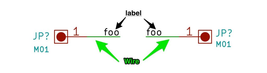
KiCad Bus, Label, and Wire
Before jumping to how to use a bus, first, we need to start with the basics. KiCad connects nodes with a “wire” element. KiCad gives each wire drawn a unique name unless it connects to an existing node. The user can override the name by adding a label.

One of the last significant steps in a project is designing the custom PCB. This stage means creating a DIY Arduino board that is custom to the application. Two examples of my past projects are BinBoo, a Binary Clock, and Open Vapors, my reflow oven controller.
While working on a project for a friend, I got to thinking; it would be nice to have a checklist for circuit elements to include on a DIY Arduino board. In the early days, I forgot to add a filter cap to AREF, for example.
These tips are based on an 8-bit AVR design, like the ATmega328p chip. You could apply these tips to other 8-bit AVRs. Until now, I have not designed a custom board around a 32-Bit/ARM board. Though at only $16, I would be tempted to just solder the Teensy module directly to my finished board.
Below is a written list of items for a DIY Arduino checklist. If you’d like to see me design this board in KiCad, check out this AddOhms Tutorial.

This screen shot is an all-layer view of my TLC5940 painter board. The 1st draft featured two TLC5940s, but I decided it made the board too large. Instead, I wanted the ability to mount the painter boards around the LED’s shadow box. This should make routing all the wires much easier.

In an attempt to find a free set of schematic and PCB tools for hobby work, I looked back at gEDA. The last time I used it was when the project first started, years and years ago. I was happy to see that OS X had a set of fink packages for the gEDA suite. After figuring out how to get X11 in Leopard (since I didn’t include it when I installed 10.5) and install fink, getting gEDA going was a snap. The user jluciani in the Arduino forums has provided some free pcb footprints he has used from previous projects.