KiCad 8 just dropped. Here’s an AddOhms video covering eight must-try features! The February 2024 release brings a whole host of new stuff to the Schematic editor. However, the PCB editor, CLI, and Simulation tools also received attention. (There are something like 900 closed issues for the 8.0.0 Milestone!) Which of these is your favorite?
During the component shortage, I got to know Raspberry Pi’s RP2040 microcontroller. It is a dual-core Arm Cortex-M0+ with about 262 kilobytes of RAM. The feature I like most is the programmable IO pins. These are small state machines that run independently of the Arm cores. They allow for some clever tricks. For example, I used them extensively on the Mega IIe project.
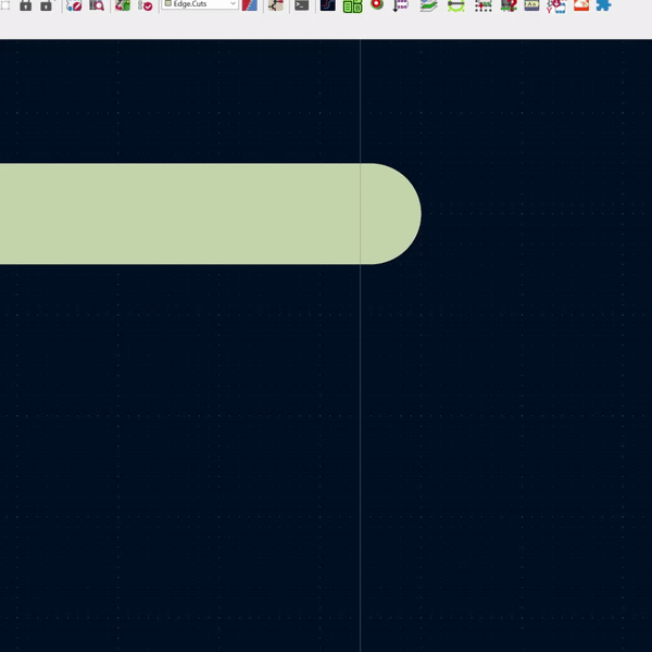
In KiCad 6, using the Polygon tool makes square boards easy. Just select the Edge.Cuts layer, then the polygon tool, and draw a square. However, if you want custom shapes, then you need to connect multiple line segments together.
If you are not careful, the segments will not connect and you might get one of two errors. The first comes when you run DRC.
Error: Board has malformed outline (not a closed shape)
or, if you try to render the board in 3D (ALT-F3).
Board outline is missing or malformed. Run DRC for a full analysis.
As the gif above shows, there is a small trick to connecting the segments. Zoom in, grab an endpoint, and then “snap” it to the other line. Watch carefully for a white circle to appear along with a purple box. Align those boxes and SNAP. Now the segments are connected together.
Measuring a switch-mode power supply (SMPS) with a DMM might show a stable voltage. But the same DC rail on an oscilloscope can show a completely different story! In this video, learn how to correctly set up an oscilloscope to characterize the noise an SMPS creates in a circuit.

In April 2019, hardware hackers, hobbyist, and engineers joined together for the first KiCon. A couple of people asked me, “why is there a conference for KiCad?” Some questioned if KiCad was significant enough software to warrant a conference. That question is valid. But KiCon is larger than the KiCad software. Even in its first iteration, KiCon evolved more into a meeting for people building electronics hardware from small scale hobbyist to professionally designed systems, than just a conference on a single piece of software. Some might call it a maker conference. I call it a hardware developer conference. The key that tied everyone together is the open source software behind our printed circuit boards.
Twenty-five different talks covered basic KiCad usage, automating tasks, PCB layout techniques, and projects designed in KiCad. Wayne Stambaugh ended the first day with a State-of-KiCad discussion. He introduced the feature list for KiCad 6. Additionally, he announced four new lead developers and that he would be working on KiCad full time. That news means it is likely KiCad 6 will be here faster than the usual two-year release cycle.
In addition to the talks, there were several workshops and panel discussions. The workshops included a getting started with KiCad lead by Shawn Hymel [link]. That one was cool to keep an eye on because people were designing their first PCB, milling it, and then soldering parts to make the boards blink. In another workshop, Anool Mahidharia provided a hands-on guided introduction to FreeCAD. It is a parametric mechnical cad tool. The panels featuerd PCB manufactureres, workflow discussions, and the KiCad development team.
Outside of the planned classes and activities, I finally shook hands with friends whom I only knew through social media. Even though we are all electronics enthusiast or professional engineers, it is rare we end up at the same place at the same time. See what I mean about KiCad connecting liked minded people together?
With so much going on, I realized I couldn’t cover everything. Instead, this post’s focus is the tidbits I learned at the conference and stuck with me after a little bit of time passed. Here are the six things I learned at KiCon 2019.