KiCad 8 just dropped. Here’s an AddOhms video covering eight must-try features! The February 2024 release brings a whole host of new stuff to the Schematic editor. However, the PCB editor, CLI, and Simulation tools also received attention. (There are something like 900 closed issues for the 8.0.0 Milestone!) Which of these is your favorite?
During the component shortage, I got to know Raspberry Pi’s RP2040 microcontroller. It is a dual-core Arm Cortex-M0+ with about 262 kilobytes of RAM. The feature I like most is the programmable IO pins. These are small state machines that run independently of the Arm cores. They allow for some clever tricks. For example, I used them extensively on the Mega IIe project.
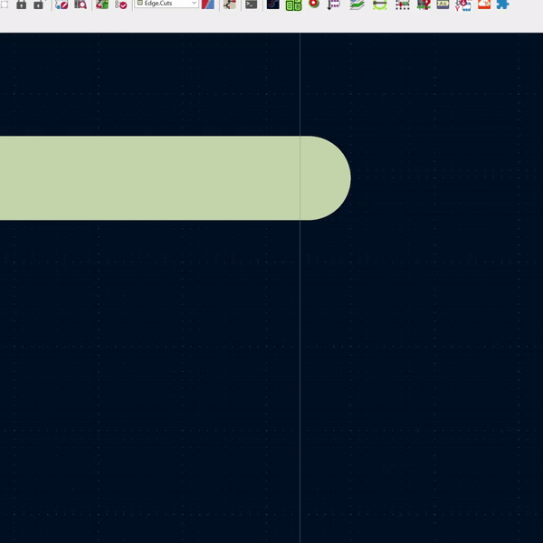
In KiCad 6, using the Polygon tool makes square boards easy. Just select the Edge.Cuts layer, then the polygon tool, and draw a square. However, if you want custom shapes, then you need to connect multiple line segments together.
If you are not careful, the segments will not connect and you might get one of two errors. The first comes when you run DRC.
Error: Board has malformed outline (not a closed shape)
or, if you try to render the board in 3D (ALT-F3).
Board outline is missing or malformed. Run DRC for a full analysis.
As the gif above shows, there is a small trick to connecting the segments. Zoom in, grab an endpoint, and then “snap” it to the other line. Watch carefully for a white circle to appear along with a purple box. Align those boxes and SNAP. Now the segments are connected together.
Measuring a switch-mode power supply (SMPS) with a DMM might show a stable voltage. But the same DC rail on an oscilloscope can show a completely different story! In this video, learn how to correctly set up an oscilloscope to characterize the noise an SMPS creates in a circuit.

A project I work on in my spare time is creating a portable Apple II. Like many of my projects, one leads into another. I started out wanting to make a mobile Apple II, and now I’m working on a project called Bit Preserve. How did I get from one project to the next? Well, as I looked into how to make a portable Apple II, I realized a significant issue. The original Apple II logic board has almost 80 ICs. Being a design from 1975, they are all through-hole packages. The good news is that except for the ROM chips, they are all off-the-shelf components. But such a size means it might be impossible to turn it into something handheld. I almost abandoned the project. Then, I learned about a chip included in the Apple IIgs. The name of the ASIC is “MEGA II.” (Nothing to do with Arduino.) It is a chip that integrates all of those off-the-shelf chips into an 84 pin package.
As I dove deeper into the project, I realized I needed other support chips to make the MEGA II useful. There is a decent book that discusses the technical details of the Apple IIgs, but it does not get into chip or board level design. For that detail, I had to look at the original schematics. While I am ecstatic that someone archived these original documents as PDFs, I quickly became frustrated. Sometimes the scan quality is not very good, and it is nearly impossible to search for symbols across multiple pages. I thought to myself, “There has got to be a better way!”