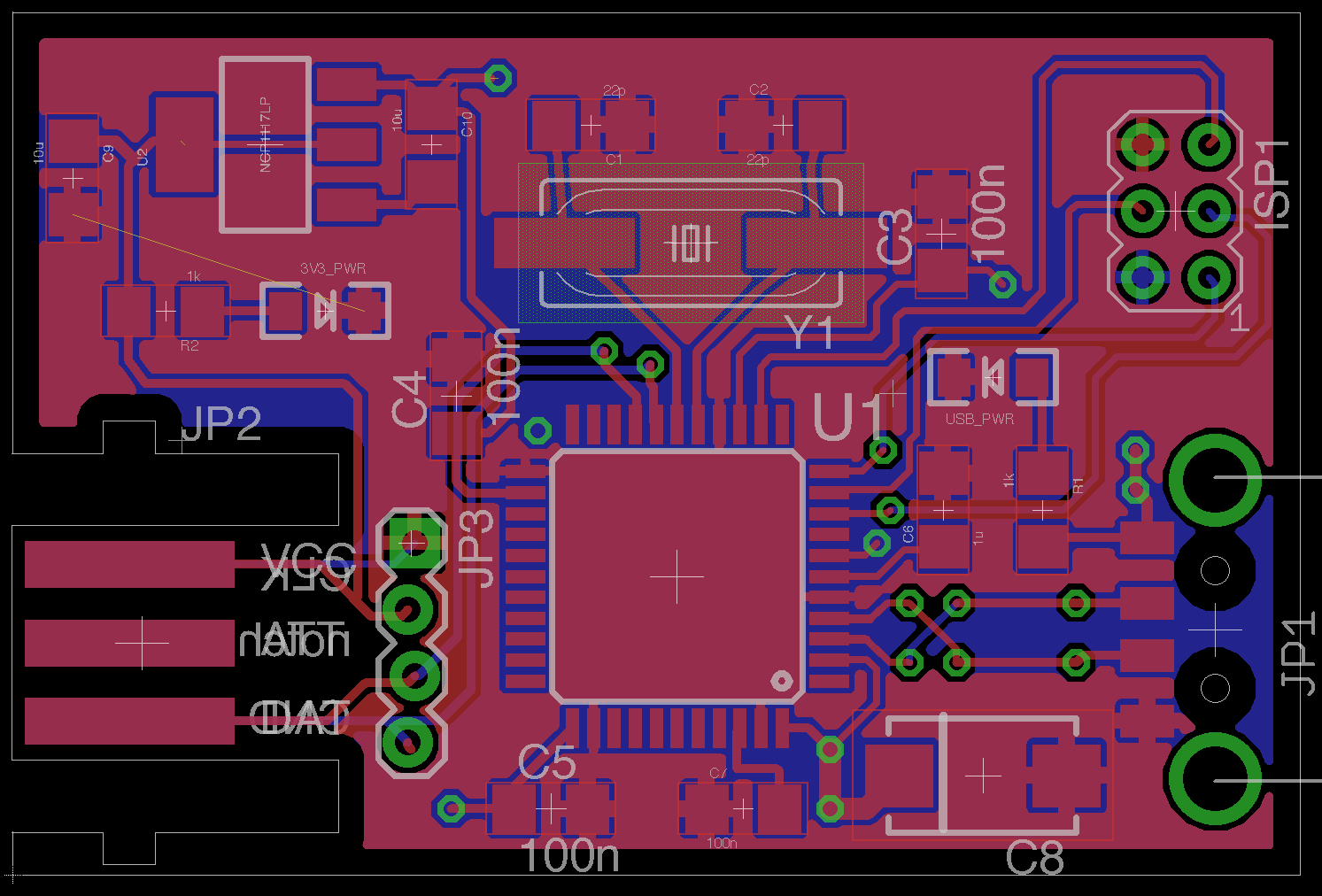
Your challenge, if you chose to accept it, is to determine why EAGLE is showing a ratsnet connection on the far left of the PCB layout. The pads shown with the yellow unrouted line are both GND. They are both surrounded by a ground plane, which is also connected to GND.
 Fills")
Creating PCBs in Eagle is a straight-forward process once you understand how EAGLE works. In fact, most users can get up to speed enough to draw a Schematic and then layout a simple PCB. Making the connections between components is not only fun but can be a form of artwork.
Often overlooked is how much space is left wide open. For example, a board might look like this:

The area in black will have no copper. For circuits that don’t require a ground plane, this may not be an issue. However, it rarely hurts to fill in empty area with a ground plane. EAGLE makes it very easy to do this, after your circuit design is complete.