
On every page of my blog, you might notice a chat window. If I’m not busy, we can chat in real-time. If not, the messages come to me by email. Here’s one I got from Matt the other day:
Let’s talk a bit about how (and why) you would use a P-Channel MOSFET. Matt, and he’s not the only one, is probably asking this question based on the “myth” that P-Channel MOSFETs require “negative voltage” supplies.
Keep reading for how-to use only positive voltage in this p-channel MOSFET tutorial.
N-Channel and P-Channel MOSFET Tutorial Video
First, for some background, check out this AddOhms video tutorial about MOSFETs, I already made.
What’s different?
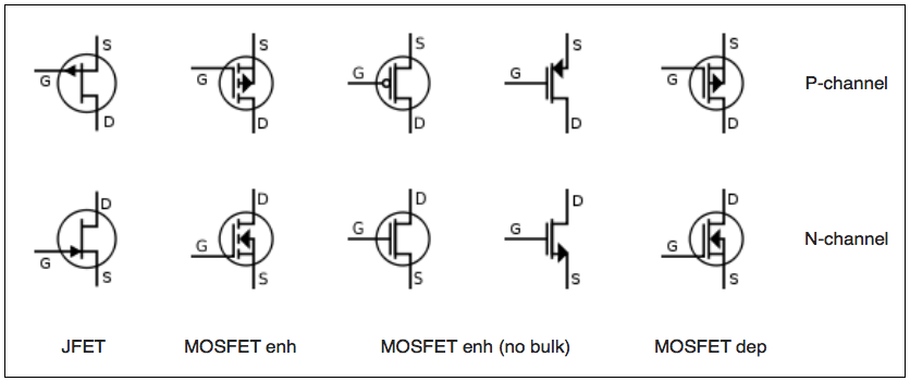
The actual construction of the two types of MOSFETs differ. There are plenty of those explanations out there on the layers. Instead, let’s focus on how you use them in a circuit.
VGS Threshold
The first thing we need to know about using MOSFETs is one of their critical properties: VGSth. Which stands for Voltage Threshold from Gate to Source. As the voltage difference between those two pins changes, so will the resistance from the DRAIN to SOURCE pins. This threshold is how a MOSFET turns ON and OFF.
How that resistance changes, depends on if it is an N-Channel or P-Channel MOSFET.
P-Channel MOSFET Tutorial and Explanation
Look at the VGSth for a P-Channel MOSFET. You might notice that VGSth is a negative value. We can use the datasheet from an IRF5305 as an example.
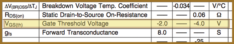
Its VGSth is specified as a range: -2.0V to -4.0V. So, how could you possibly use this MOSFET with an Arduino, LaunchPad, Raspberry Pi, or any other microcontroller? Do you really have to generate negative voltages?
It’s about the difference
This spec is where the myth of the “negative voltage” comes in: Since the datasheet says negative, clearly, you need negative voltage to work. And datasheets, never lie (except when they do…).
Let’s literally read what the specification is saying. “Voltage from Gate to Source of negative four volts.” Using different words, you might read it as “GATE voltage value minus the SOURCE voltage value.”
Look at the voltages in this “high-side switch” configuration:
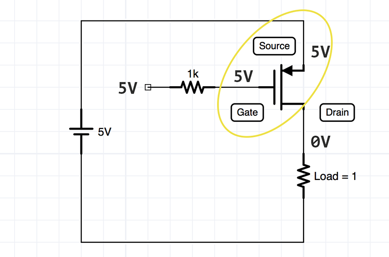
The GATE is now at 5 volts. The SOURCE is also at 5 volts. That means the Vgs is 5V – 5V = 0V. So the Vgs, in this case, is 0 volts. This voltage means the MOSFET is turned off, or an open.
Now, this is the same circuit, but the GATE is connected to ground instead of 5 volts.
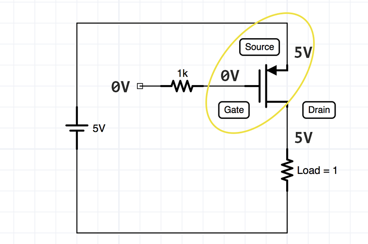
Let’s look at the SOURCE and GATE again. The SOURCE is still at 5 volts. However, now the GATE is at ground which means it is 0V. If you take the GATE voltage minus the SOURCE, you get 0V – 5V = -5V. This will turn the MOSFET on.
See what just happened there? We got a “negative” voltage using only positive voltage supplies…
Why use N-Channel over P-Channel
We would need to dedicate a tutorial on when to use an n-channel and p-channel MOSFET. An excellent use for P-Channel is in a circuit where your load’s voltage is the same as your logic’s voltage levels. For example, if you’re trying to turn on a 5-volt relay with an Arduino. The current necessary for the relay coil is too high for an I/O pin, but the coil needs 5V to work. In this case, use a P-Channel MOSFET to turn the relay on from the Arduino’s I/O pin.
If your load voltage is higher, like 12 or 24V, then you might want to use an N-Channel MOSFET in a “low side” configuration.
Conclusion
Using a P-Channel with positive voltages is easy when connected to the circuit correctly. We just have to get over the myth that they work with “negative voltages.”


92 Comments
James,
Not sure you are still monitoring this page but your expertise would be very useful. I am using a P channel mosfet (IRF9540N) as a switch for a sensor system. The gate is controlled via the square wave output alarm system of a DS3231 RTC clock. The gate and source pins are bridged with 1k ohm resistor. The drain pin is connected to my Arduino. When I supply power to the source pin with a 9.6V series of AA batteries (2000mAhr) the system works fine, every half our the RTC square wave closes the MOSFET and the system powers on and then turns off after my measurements are completed. The problem has come when I’ve tried to increase the voltage and Ah to extend the battery life of the sensor. I would like to use a Li-ION battery with a 12.8V output and 7Ah. The MOSFET remains on continuously and does not respond to the RTC square wave. Is there a simple fix for the system (maye the 1k resistor isnt enough or too much) or do I need a new MOSFET? I apologize if this isn’t completely coherent, I’m not necessarily and expert. Thank you in advance for your help.
The capacity (Ah) of the battery is irrelevant.
If you increased the Source pin’s voltage and it isn’t turning off, then make sure you are pulling the Gate’s voltage up to 12.8V.
Just wanna say thank you for this elaborative explanation. Very simple, straight to the point and insightful at the same time.
thank you for a very good little explanation…!!! NOW… I have a 37 volt power supply.. I believe that I have to use a P-channel FET.. to be driven by the output transistor of a MC34063.. switch chippy.. the problem I have is the resistor I need across the DRAIN to GATE of the power P-channel MOSFET. I using IRF4905… so the output of the MOSFET.. is to drive a diode – coil – and cap.. so that I have a step down converter.. using the MC34063… I want to know what value resistor I should be using across from DRAIN to GATE…?? I hope that a 220 ohm 10 watt resistor should work.. and that the P-channel MOSFET .. is turned on.. hard enough .. the circuit is basically described above.. there is a 10 ohm resistor from GATE to the open collector of the MC34063. The emitter of the MC34063 chippy.. is grounded .!! So that when the MC34063 output transistor is turned on.. the GATE of the P-channel MOSFET.. is dropped to about 0 volts.!! This should totally enable the MOSFET .. and hopefully when this happens the RDs of the MOSFET is very low.!!! and so heat dissipation in the MOSFET is very low.??? so basically there will be almost 37 volts across the 220 ohm 10 watt resistor.!!! DOES THIS VOLTAGE ADVERSELY AFFECT THE VGS LIMIT OF THE MOSFET.??? Hopefully when the “bottoming”.. of the GATE voltage is removed.. MC34063 is switched off… the GATE voltage will become almost 37 volts.!!! and the MOSFET should be turned off.!!!
which circuit would you suggest rather.?? using this P-channel .. OR rather a saturated N-channel.. driven by the emitter output of the MC34063.. with the collector tied to 37 volts.??? so that the GATE of the MOSFET is hard driven ON..!! by the MC34063…?? Please advise.. ??? I think possibly the saturated N-channel circuit would be better.. in this step down mode.. since the input to output voltage differential is so great.!!!
I await for any answers.. please .???
thanking you.. George…
Between the scatterbrained explanation and the ridiculous punctuation, I cannot even remotely understand what is being said (or asked?)
Hello James,
I don’t know if you are still working with this web page or not. I just wanted to reach out and ask you a question.
My Vcc for the G pin will be coming from a “rasberry pie” and my power for the D pin is coming from a power source of 12V DC. I activating a door lock. (I believe that it’s a solenoid). I have the N-channel MOSFET in the “low side configuration” and when I hook up the power it turns itself on. Not certain what I’m doing wrong. I’m thinking I need a resistor somewhere. Any help would be great.
Sounds like you need a pull-down resistor from Gate to Ground. Something between 1K and 10K. The value isn’t critical.
Between the time you responded and the time that I wrote my question I had been doing some research to remind myself of the answer. I am very happy that you responded with an answer so quickly. I was on that path already, but before I had a chance to test my thoughts you answered and confirmed what I was thinking. Thanks again for responding so timely. I get to end my day on a very “high note!” My circuit works great and I get to help a friend out with a business project that he has been working on for a while. He needed my circuit to complete the process.
Have a great rest of your memorial holliday!
Very clear – Tks for the example of circuit- it helps to understand
I ran across a site where a fellow designs motor control systems and also makes his motors over seas, I looked at his circuitry, more than one, in which he shows parallel MOSFET bridges. It looks confusing the way he has them illustrated. To me it looks like he is using both N and P channel FET’s. What I am wondering is he simply drawing the schematic incorrectly or can this actually work this way? The web site is about BLDC motors for go karts and such. I am still trying to get on his site to ask him but haven’t been able to get anywhere yet. I’m not an electronics engineer but do have background and I like to build stuff. In this case it is looking more appealing to simply purchase a controller to start with and work on building my own later.
Hi,
I am working on a little project where I need the Led “Normally On ” but it will turn off when I apply the positive voltage (+12V) until I remove this +12v and the led will turn back ON again. What kind of MOSFET do you recommend ? Seems like this tutorial will work for my application too but just want to make sure prior to purchase this P channel mosfet. I guess I need the P Channel Depletion Mosfet . Thought ?
Thank you for your great post and video.
But how we are going to drive the MOSFET if the supply voltage of the load is way higher than the 3.3 or 5 volts of logic?
For example if we have a 50 volts fan as a load, and we want to drive it by a P-Channel mosfet, we need 50 volts on the gate of the mosfet to keep it off, and something below 50 to turn it on, if I am not wrong.
I thought I could use a BJT to switch the 50 volts to the gate, but when I want to turn the mosfet ON, the BJT should be OFF so the Gate of the mosfet becomes zero volts, and there will be -50 volts VGS that exceeds the maximum allowed VGS of the mosfet (20 volts typically).
So how can I switch a high voltage with a P-channel mosfet as a high side switch?
Perfect tutorial…. I am trying create a simple circuit for switch, 2 source power, when the main power is 0V or disconnected would like put other source power, from battery lipo. I am using mosfet P channel, because i would like know when the main power supply is 0V for turn on other source power. When i place this circuit in protoboard for test.i can see that power supply main return in the mosfet, going this voltage for other side. Everbody say that inside mosfet there are a diode, So this energy cant back for other side, if a measure with multimeter i can see voltage reverse. what way correct for switch 2 power supply without current or voltage reverse? thks
Hi, have a look at one of Adafruit’s circuits for the Feather, they are doing exactly that. It boggled my mind for a while, as I know what the circuit should do, and when I simulated it in LTSpice it gave the correct values, I just couldn’t understand how it worked. But you can use it as a reference.
https://cdn-learn.adafruit.com/assets/assets/000/041/630/original/feather_schem.png?1494449413
“Why use N-Channel over P-Channel
We would need to dedicate a tutorial on when to use an n-channel and p-channel MOSFET.”
I understood the description of your example but only got the label “in this case use p chan” but I wasn’t sure why. So if you do get a chance, a tutorial/deeper explanation of why p is better than n and then any further explanation would be superb.
Thanks so much for your explanations so far and in particular how to understand/what to look for in the datasheets. You’ve really helped! A great teacher indeed!
A simple rule but definitely not inclusive is P is for Positive N is for negative switching. For discussion we will assume a 10V system (keeps the gate circuit simple). If you are doing a high side switch (pulls the load high or positive to turn it on) a P-channel device would be chosen. Conversely if you are doing a low side switch (Pulls the load low or to ground) an N channel device would be chosen.
Consider the source as the input and the drain as the output. For a P-Channel device with the source connected to the + you drive the gate to the ground. Pull gate to source to turn it off. The opposite is the N-Channel device, it switches the – side (typically called ground), you drive the gate + to turn it on. As before the source is the input and the Drain is the output. Please note these devices have an intrinsic internal PN junction which acts as a diode. If source and drain are reversed it becomes a diode where the voltage drop is based on the channel resistance, not a fixed voltage.
Yes they can be used as diodes with typically a lower voltage drop then a diode. You will see them used this way in some low voltage high efficiency power systems. This internal “diode” is “ruggedized” in many devices and is designed and tested to withstand a UIS (Un-Clamped Inductive Spike). Some manufacturers test this parameter on every device. This is saying it can replace the fly back diode in most applications. Remember when an inductor discharges it reverses polarity and allows the voltage to climb until limited by some external means. The substrate diode (PN Junction) will clamp this to a few hundred millivolts. This PN junction is a basic part of the MOSFET structure not added later.
No mater which way you connect the source and drain the MOSFET will conduct, if it is reversed you will not have any control with the gate, your choice. I am not going to get into it here but there are many different circuits with and without charge pumps that can for example use a N-Channel device as a high side switch.
I like the simplified idea of “P is for Positive” and “N is for Negative.” I might use that in the future! 🙂 Thanks for the comment.
“P-Channel MOSFET Tutorial with only Positive Voltages”
Why use N channel devices to illustrate P-Channel MOSFET Tutorial with only Positive Voltages?
It’s a P-Channel. Annoyingly, this symbol style is drawn with the error opposite of other symbol types. It is an IEEE standard symbol.
Explained better in this tutorial on high-side and low-side switches.
What is commonly missed is where the reference point is. That is the point where you base all your measurements. The polarity of a MOSFET is referenced from the source. That is where you would connect the ground of your volt meter. Doing it that way the datasheet is correct regardless if P or N channel. Simply think as the black wire or ground is your reference point. It always works for me.
Thanks a lot for this detailed explanation ; would you have any idea of how it works at the level of the electrons flow? this is because we always see the drawing of the P-Channel where they say that some negative charges are needed at the gate to push the electrons away and cut the flow. I still can not figure it out in a CMOS when the same direction current can both apply negative charges on the P and positive ones to the N. I’m sure that my question is silly but forgive me I’m just a biologist with some interest in electronics…
You’re confusing voltage polarity with electron charge. Electron charge is always negative. In a semiconductor, there are charge carriers in a channel. The voltage (electric field) changes channel, enabling the carriers more mobility. In a P-Channel, a negatively biased electric field is necessary for the channel to become active. That “negative” has nothing to do with an electron charge. Nor does the voltage have to be “negative.” The voltage at the gate just has to be less than the voltage at the source, thus creating a “negative voltage” when looking from Gate to Source.
While performing a diode test with a multimeter (red probe on Source pin and black probe on Drain pin) on an stand-alone (not in-circuit) NMOS, I get a 0.5V reading which is expected. However, when the NMOS is placed in-circuit (soldered onto PCB) where the Source pin is connected to ground plane, I get 0.135V. Circuit is not live. Is the 0.135V to be expected or should it read 0.5V?
I’m wondering if the 0.135V reading is valid due to the Source pin being connected to ground plane or if it is a botched soldering job.
Sorry for the newbie question, but what exactly does the resistor on the gate do? I’m connecting the gate to an arduino so guess I’d need that resistor in between the gate and the arduino, but I’m not sure what it does. Thanks in advance!
The gate of a MOSFET is a capacitor. Depending on the size of the FET, that capacitor can be large enouogh to cause damage to an I/O pin. So the transistor limits the current. Anything between 100 to 1000 ohms works fine.
Wow, a really great tutorial. Thanks.
In the whole of my learning about MOSFETS, I could not see just how the gate of a p-channel MOSFET could possible be a negative voltage value – to turn-on the MOSFET. For almost a week of searching ‘other’ sites for more information, I stumbled upon your great explanation! Your Tutorial really highlights an issue that would cause deep frustration in many electronic Hobbyists. So thankful that I stumbled upon your Tutorial. Greetings from Australia.
“Using different words, you might read it as: subtract the GATE voltage value from the SOURCE voltage value.”
I think you mean the reverse. In your second example, your statement shows 5-0 which is +5. You want gate, 0, minus source, 5. So -5. Subtract gate off source.
Other q. Using arduino i/o, 5v high. Source is 12v. I imagine the Vgs is either -12 or -7 hence, always on? (P chan config). Guessing I need a transistor before the gate, to send 12v to the mosfet, thus inverting how I drive it (with a low)?
I’ve finally realized a way to re-word it just using “Minus”instead of subtract.
It’s called a “driver.” This post has an example where I drove a PNP transistor with a NPN driver. Also, just a minor point, you never “send” voltage, you can only “apply” it.
True about apply. Same with a Low, it is not a send, rather, a sink.
Great edit on the wording change. MUCH clearer now. 🙂
I bought a whack of N Chan boards for my arduino, was going to use on the truck’s headlight LED rings and other. Problem is, I cannot get to the neg, ergo, ground, to make it a Low side N chan circuit to work with those mini boards. The ground and source are also bridged on those. I May unsolder the mosfet, try a high side with that N using 12v.
Cheers
Hi, Very nice addohms video as usual. I have a logic level n-channel mosfet(FQP30N06L) and switchin on-off by appliying 0 and 3.3v Vgs from a gpio pin. Drain side I have a load operates at +5V. After the pc turns off, PC pulls up +5V all GPIO pins(Vgs). As a result after pc turns off, it turns on the load again. How can I prevent the gate voltage if more than 5V at the logic level mosfet? Best.
I don’t understand your question. You may need to use a P-Channel FET as a high-side switch. Or you may need to add a pull-down resistor to the N-Channel’s gate.
Thanks for the reply. Let me explain again. We simply control a load by using a gpio pin on the gate side of mosfet. From the industrial pc software, it gives 3.3 and 0 volts for high and low to the gate. But when we shut down the industrial pc, it pulls up all gpio pin to 5V(we dont know why) I would like to prevent the load to turn on if the gate voltage is higher than 3.3volts(it can be 4.5V also according to vgs threshold). Hope this is clear. Best.
If your driving signal tends to float high, I would suggest replacing the circuit with a p-channel high-side transistor. On the N-Channel, you could also try using an NPN to invert the driving voltage.
In this circuit when the input to the NPN base is high, it will turn on, which puts 0 volts on the gate of the MOSFET. When the NPN’s base is low, it will turn-off, putting 5 volts on the gate of the FET.
To be honest I dont think the diagram above should work high logic signal at the gate since it floats between 3.3V and 5V. It is ok to control with 3.3V and 0V but not ok with 5V. We dont want to current flow to the load(5V, 2A) at 5Vgs on mosfet(FQP30N06L). As you said (also in my opinion) a P-channel transistor might be placed. According to diagram we get 5V high from the plc after shut down which activate npn either way. Also you can think the load is the 1k resistor at the right hand side. Briefly we need a transistor doesnt turn on above 3.3v at the gate. Many thanks.
Thanks a lot for this article. One point has me confused. Early on, you mention:
“Let’s literally read what the specification is saying. ‘Voltage from Gate to Source of negative four volts.’ Using different words, you might read it as: subtract the GATE voltage value from the SOURCE voltage value.”
But subtracting gate voltage from source voltage is Vs – Vg stated mathematically, and it is the opposite of what you do in your examples.
Funny enough, the way you stated it verbally makes more sense than Vg – Vs. When I think “from point A to point B”, I tend to think B – A, not A – B. For example, if A is 3V and B is 5V, to get from A to B, I need to add 2V, so Vab = 2. I’m just so extremely confused with notation because this isn’t the first place where I’ve read about MOSFETs and saw that Vgs = Vg – Vs. It just makes no sense to my mathematical mind why it seems to be reversed.
Can you help illuminate?
I’ve given up trying to explain it in words. I’ve changed it 3 times in 3 years and people still say it is confusing. So far everyone’s “clarification” confuses someone else. I think it comes down to how you process math in your mind. So, Vgs = Vg – Vs.
I don’t have the project with me any more. It was a gift for a friend who was going away, but I do have all the parts and one of the FETs mounted on an SMD to DIL PCB. I will make up the circuit again on a breadboard and play around with it. If I come up with something, I’ll post it here.
When I did the original project I had limited time so as long as the theory was solid (based, actually, on your explanation, thanks) and the completed project worked for a few hours without any heating I was happy.
Thsnks for this most informative blog. It helped resolve a problem I had with the P-channel MOSFET AO3401. I connected it in exactly the same configuration as in your last circuit with an additional 10K resistor between gate and source. The input went to a CMOS IC and the load was parallel LEDs totaling 120mA. It always remained ON irrespective of the CMOS output being high or low.
If I disconnected the 1K from the CMOS output, connected it to a transistor collector and the transistor base (via a resistor) to the CMOS input, emitter to ground, the LEDs switched on and off with the CMOS output.
I had limited space. I didn’t want to use a transistor.
I ended up connecting the circuit exactly like yours, but with the load between the 5V supply and the source of the AO3401, drain to ground. It worked!
My logic is that since it is a series circuit the MOSFET should handle the current whether the load was in the source or in the drain. My question is: am i right and will there any problems with the MOSFET connected in this way. The reason I ask is I googled a lot of P-Channel MOSFET schematics, but I never saw one connected this way.
That’s creating a “low-side” switch. Usually, a P-Channel will be configured as a “high-side” switch as I show here. However, it just comes down to the voltage difference between gate and source.
The current isn’t an issue in either a low-side or high-side circuit. It comes down to the voltage difference between gate and source. Without a schematic, it is hard to evaluate if your circuit should work as expected.
Thanks for taking the time to reply to my enquiry. Sorry about the delay in my reply. I was looking for a good way to make schematics on my phone. I found a very nice app. I’ve uploaded my schematics to dropbox so that you can have a look. The link is here: https://www.dropbox.com/sh/v139ctjkrcm6d45/AACG_kwgV25Zk4QblPQCmJTya?dl=0.
The TTP223 I/O terminal can only handle 8mA so you need a driver to switch LEDs. I wanted to mount the driver on the 11x15mm sensor board. There was just enough space for one SMD MOSFET and resistor on the touch plate side.
In Fig1, the LEDs remain permanently ON, no matter what the I/O voltage is. In Figs 2 & 3 they switch ON/OFF with the change in I/O voltage.
I measured the I/O voltage and in all cases the high/low swing was 0V to 5V. You can set the jumpers on the sensor board for high on or low on, momentary on or latch on. The I/O terminal is specified as CMOS [probably similar to the push-pull kind of arrangement available in CMOS gates] as opposed to open Drain available in the 16-pin version of the IC.
I was puzzled with the result from Fig1 because I expected the FET to conduct only when the gate voltage came down to near ground voltage, but in this case it was conducting all the time.
I have already completed my USB touch activated night light using Fig3, but I’m still not sure why Fig1 didn’t work. Thanks again for your help.
I’m not sure why it is staying on, I would expect Fig 1 to work. However, I would have implemented with figure 2. I would not have expected figure 3 to work at all.
I don’t see how your last circuit could work as drawn. Since the Vgs in a P-channel MOSFET must be negative to turn on, and the source pin is held at ground, the gate can never go negative with respect to it since it only provides +5v or ground. That is why P-channel MOSFETS have the source pin tied to the high-side load–so that Vgs can be negative. Were the drawn circuit using an N-channel MOSFET (with the source tied to ground), or the P-channel MOSFET reversed with drain to ground, then I could see it working.
For that matter, the first circuit drawings that describe the negative Vgs (using only a positive supply) for a P-channel MOSFET are drawn using N-channel MOSFETs. Based on the circuit, it looks like it is a ‘typo’ where the arrow is pointing the wrong way (for a P-channel MOSFET).
Every circuit drawn in this post uses a P-Channel symbol.
For some reason, the way that the ‘MOSFET enh (no bulk)’ symbol is standardly drawn is the opposite of every other FET symbol: the arrow on the source points into the P-chan device instead of out. Most confusing. (Reference the Wikipedia drawing.) Other standards (e.g. JEDEC and IEEE) aren’t real consistent either. The one you chose to use is an ‘outlier’ to the most commonly used symbols that I have encountered—in terms of arrow direction. Because of the potential for confusion, I think the best approach is to explicitly state what the source of symbology is (which you did) and explicitly state whether your symbol is P-channel or N-channel (on the drawing). Including a note to the unwary in a tutorial that the arrow direction is ambiguous would be a good idea, too. When designing with actual FETs, use the symbol used on the manufacturer’s datasheet for the part you are using.
Thanks for your opinion. I have no plans to change this post or its graphics. So far, only 1 person has had an issue understanding the schematics (out of hundreds of thousands.)
The source is tied to 5 volts in every schematic in this post.
The diagram with the NPN transistor buffer does show the source tied to ground, not 5v—the source being the lead with the arrow on it.
If you’re talking about the comment from Nov-21, it is an N-Channel.
Great article! For a battery powered ATtiny project I have been using a low-side configured N-channel enhancement mode MOSFET to turn on and off a circuit so that the whole product draws just a few microamps when in sleep. A new requirement is that the circuit is turned on and off on the high-side. A single P-channel MOSFET configured to the high-side seems like it is on the right track but requires that the pin be set high to turn off the circuit so that won’t work to keep the current usage to near zero when in deep sleep. I need to keep the cost and parts count low and would really appreciate any ideas you have on this.
Thank you profusely sir, for explaining so simply yet to the point
What happens if we provide negative supply to the p mosfet? How to turn it on? Do we need a level shifter?
The voltage from gate to source needs to be negative. It does not need to come from a negative supply.
Suppose we want to run it with a negative supply then how should we level the voltage of gate?
I don’t understand what you mean. I don’t understand “run with negative supply.” A transistor is a simple switch.
I mean if we provide say -12 volts to the source and ground the drain. In this case, how to turn the p mosfet on?
Thank you.
Please how do I identify n channel and p channel mosfet on laptop motherboard. Reply asap
If you cannot identify the part from its markings and you do not have a schematic for the circuit, you will probably need to remove it. From some basic testing, you can determine if it is N or P, but you probably can’t determine an appropriate replacement.
I was searching for more information on how the P channel was different than the N channel but nowhere did I find such a great explanation as this page.
Yes, I was confused by this as well.
what happens is your gate value is bigger than the source? does still operating?
Nope. In that case Vgs would be a positive voltage, so the p-channel would not work.
Hello sir we are trying to make H bridge inverter using 4 N channel MOSFET. But when we triggered the gate pulses simultaneously only negative voltage output waveform is fine. But in positive voltage the voltage is too short than Negative voltage. Is there any need to change the positive side N channel MOSFETS to P channel?
Thank you.
Hello,
I have an TP0610K P Channel Mosfet –> VGS – 1 to – 3
And i get on a laptop motherboard (black probe on gnd)
Source -> 19V
Drain -> 19V
Gate -> 3.3V
The gate shouldn’t have 19v- 3v ?
Sorry for a newbie question 🙂
The threshold value given, VGS, is the minimum needed to activate the FET. In the absolute maximum section of the datasheet, you’ll see the maximum value of Gate – Source. 3V – 19V = -16V.
Nice article, but the phrase below seems backwards to me:
“The SOURCE is still at 5 volts. However, now the GATE is at ground which means it is 0V. If you subtract the GATE from the SOURCE you get: 0V – 5V = -5V. ”
If I subtract GATE (0V) FROM the SOURCE (5V), shouldn’t that be read as “5V-0V”, not the other way around?
Thanks
I think the source of confusion is the earlier sentence “Using different words, you might read it as: subtract the GATE voltage value from the SOURCE voltage value.” If it read “… subtract the Source voltage value from the Gate voltage value.” then it would be consistent with math examples that follow.
Does this device just swing from hi to low, or will the drain voltage follow a varying gate voltage?
That behavior isn’t defined by N or P channel types. A JFET’s drain voltage will vary with the gate voltage, in the ohmic (or linear) region of the transistor. Enhancement mode FETs will as well, but their range is extremely limited. They’re really designed for operation in the saturation region. Here’s a good app note on the subject: https://www.vishay.com/docs/70598/70598.pdf
12v or 6v on board and 5v in Proteus simulation
If I have a Source =12V (P mosfet) Drain – Load – Negative power so Vgs just 8 to 10v (because 10-12=-2 or 8-12=-4v ) I will be not connected the Gate to 0v or Ground, Do I do correctly? thank so much
I have a problem with Mosfet P channel when I assembly load on Drain and connect Source to Vcc make 0v at Gate :result fail . when I simulate a mosfet P channel (IRF9540N) with a Load on drain and run project : Result fail. Why? please tell me how to use Load in case P channel and bias of Vgs ( in N channel case is very easy) thank a lot
What is the Gate Voltage you are using?
12v or 6v on board and 5v in proteus simulation , how ever I try bias the Gate by 2 Resistors 0ne is 2k and other is 10k to fix voltage at G is 2V but proteus still get note: error and fail. I have seen more twice your video but when I simulate P channel mosfet it is fault. could you make a video about P channel mosfet and how to assembly Load (as a PNP bjt) and calculating parameters with Load : battery, Cell,(heavy load). finally thank you so much!
I don’t know why it is not working for you.
What if im make H bridge with all N Channel connected to arduino ? it is possible ?
I don’t have a lot of experience designing a discrete H-Bridge. Except for school, I’ve always used an IC.
Hello everyone!
I would like to make a switch to use a screen. My aim is to use a screen with Raspberry Pi. When the Raspberry Pi is booting, the screen is turned off. After that it will work. I need a mosfet to use it. As you know GPIO ports on Raspberry Pi have 3.3V. When 3.3V exists on the GATE, the screen will be turned off. When 3.3V doesn’t exist, the screen will work. How can I do this?
P.S The screen needs 5V and 0.8A.
Please help me. Thank you in advance.
Hi, i try to use pchannel mosfet on highside with 28v rail. And if i use npn with the base connected to my arduino. When logic is high, npn will drain everything to ground and the misfet vgs will be -28 but the problem is misfet maximum vgs is +-20v
What should i use then? If u can give a drawing will be better to understand. Thank you
Sounds like you need a voltage divider.
Very helpful. i got a PA102FDG from a PC motherboard and i was wondering how to use it for high side switching. Thank you
Just like I showed in this tutorial.
I am still confused about when to use N or P. Every example I see on the net is using N-channel by switching the 0V, which leads to load. Is it safe to say that N-channel is always switching ground, can we bring positive voltage to be switched?
In one of the comments you say that we should use N-channel MOSFET if our switching voltage is larger than the command voltage. I have similar scenario like that, I have a command ouput which when 1 (5V Arduino) should allow 12V to the load. The load in question is another input on another device, which needs 10+VDC to become high. I have no control of the load’s ground (0V).
I did not realize that Vgs threshold is actually the difference between gate and source voltage, I though it is the minimum voltage that needs to be brought to gate (disregarding the negative sign). For this reason I have bought a lot of these MOSFETs (http://pdf1.alldatasheet.com/datasheet-pdf/view/123973/TSC/TSM3401CX.html), but as it appears, this transistor keeps source-drain switch always closed, no matter if high or low signal is brought to gate. Due to your explanation it is logical to behave like this, since the voltage difference is always larger than the threshold.
So, what kind of solution do I need to make this work? When high signal (5VDC) on Gate, switch should allow 12VDC to load, when low, switch opens? Since my load is another input, required current is not large (20-30mA max).
Thanks,
Goran
If your current is that low, you might consider a NPN transistor instead. If you stick with a MOSFET, you need a “logic-level” MOSFET like the FQP30N06L.
Thanks – this really helped me use a p channel mosfet in my circuit protection design.
What I don’t understand is that you show the MOSFET is turned on with either 5 volts or 0 volts on input.
it turns on with 0V and turns off with 5V
Using a AO3401 with VGSth -0.9 gate to 3.3 volt Arduino 550Ω to gate 5 volt to source, will there be smoke?
The specified value is the minimum necessary to turn it on. The absolute maximum for the part is 12V