24 Results

kicad

Search
2020-04-04: This tutorial is based on KiCad 5. With KiCad 6, the bus feature works a little different (so I’m told.)

When your schematic has a large number of related signals, it is helpful to group them. In its schematic editor, KiCad has a few tools to help. Your end-goal helps determine which tools to use. For example, do you need a KiCad bus or a label? In this post, I explore how you can define signals, group them, and reference them across schematic sheets.

Up until recently, I did not need to use a bus or multiple sheets. However, the Apple IIgs project I’m working on is too large for a single page. In a KiCad live stream, I looked at how to create busses and connect them. In a separate tutorial, I will show how to work with multiple sheets in KiCad.

tldr; KiCad does not require the use of a bus to connect signals together. Wire labels already provide that connection. A KiCad bus offers two things: 1) a visual representation and 2) an easier way to create global connections (across sheets.)

Lastly, if you are not familiar, KiCad is an Open Source eCAD tool. Although I have used others, this one currently my preferred platform.

KiCad Bus, Label, and Wire

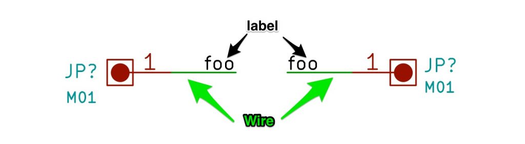
Before jumping to how to use a bus, first, we need to start with the basics. KiCad connects nodes with a “wire” element. KiCad gives each wire drawn a unique name unless it connects to an existing node. The user can override the name by adding a label.

KiCad Wire and Label Example
Wire and Label Example

A new project I have started working on involves the Apple IIgs. It was Apple’s last 16-bit (and 8-bit) computer. Inside are many application specific integrated circuits, or ASICs, that make the IIgs an extraordinary member of the Apple II family. One chip, in particular, is called the “MEGA-II.” This chip takes all of the individual logic chips from the original Apple II design and incorporates them into a single 84-pin PLCC.

The project I have in mind needs the MEGA-II. I need to design some printed circuit boards for it and a few other IIgs chips. That goal means I need at least one custom Kicad schematic symbol. I plan to create a custom library of Apple IIgs components.

Like other computers from the same era, complete schematics are available. However, they are not in a modern format. Since I need to create symbols for so many of the chips as it is, I may end up re-creating the entire IIgs schematic.

For now, here is the process I use to create custom KiCad schematic symbols and parts.

There is a project that has been sitting on my “to do” list for too long. My lab notebook has several dedicated pages for it. But I have not made progress. I decided to take some advice I have given to other people. When you’re stuck on starting a task, break down the project until you find a piece small enough you can get it done with no problem.

The project involves the Apple IIgs. It was Apple’s last 16-bit (and 8-bit) computer. Inside are some application specific integrated circuits or ASICs that make the IIgs. The name with my attention is named “MEGA-II.” It takes all of the individual logic chips from the original Apple II design and incorporates them into a single 84-pin PLCC.

MegaII from AppleLogic 960px
Image from Applelogic.org (Full)

A KiCad BOM is a list of all the parts your design is using. The term BOM, or bill-of-materials, is standard for supply chain management and does not just apply to electronics. KiCad’s eeschema has a BOM export feature. Unfortunately as of Version 4.0, this feature is still somewhat lacking. Given the limitations, here are some tips to take your KiCad BOM from Schematic to Mouser.

Spending a few extra minutes while capturing (drawing) your schematic thinking about your KiCad BOM can save you a ton of time later on. Moreover, as you build up a database of parts, these extra minutes turn into seconds. Here are a couple of ways to describe your parts, especially passive components, better while drawing schematics in KiCad.

The last time I looked at using an X-Carve for Printed Circuit Boards (PCBs), I created a demo board with EAGLE. Since then, I have learned more about using KiCad, the open source electronics CAD suite. While not a step-by-step tutorial, here is my rough KiCad to X-Carve PCB workflow. These are just the high-level steps, the tools necessary, and the settings I’ve discovered for each—so far.

Eventually, I will make this a more detailed KiCad to X-Carve PCB tutorial, so make sure you subscribe to my RSS feed for updates.

Here’s the Basic Steps:

  1. KiCad: Draw Board
  2. KiCad: Plot Gerbers
  3. KiCad: Generate Drills
  4. pcb2gcode: Generate G-code
  5. Text Editor: Clean Up G-code Files
  6. Camotics: Simulate G-code
  7. ChiliPeppr: Send G-code and control X-Carve
  8. X-Carve: Make the boards!